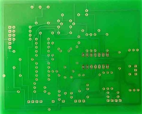
Hdi pcb design
Advantages Of HDI PCB Design In Modern Electronics
High-Density Interconnect (HDI) Printed Circuit Board (PCB) design has emerged as a pivotal advancement in the realm of modern electronics, offering a multitude of advantages that cater to the ever-evolving demands of technology. As electronic devices continue to shrink in size while increasing in functionality, the need for more efficient and compact circuit designs has become paramount. HDI PCB design addresses these needs by providing a solution that enhances performance, reliability, and design flexibility.
One of the primary advantages of HDI PCB design is its ability to accommodate higher component density.
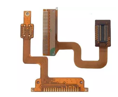
By utilizing finer lines and spaces, smaller vias, and capture pads, HDI technology allows for more components to be placed on a single board. This increased density is crucial for modern electronic devices, such as smartphones, tablets, and wearable technology, where space is at a premium. Consequently, HDI PCBs enable manufacturers to produce smaller, lighter, and more portable devices without compromising on functionality or performance.
In addition to supporting higher component density, HDI PCB design significantly improves signal integrity.
The shorter distances between components and the use of microvias reduce the inductance and capacitance effects that can degrade signal quality. This is particularly important in high-speed applications where maintaining signal integrity is critical. As a result, HDI PCBs are well-suited for applications that require fast data transmission and high-frequency operation, such as telecommunications and advanced computing systems.
Moreover, HDI PCB design enhances thermal management, which is a crucial consideration in modern electronics.
The compact nature of HDI boards allows for more efficient heat dissipation, as the shorter paths for heat conduction facilitate quicker thermal transfer. This improved thermal performance helps prevent overheating, thereby increasing the reliability and lifespan of electronic devices. In industries where devices are subjected to harsh operating conditions, such as automotive and aerospace, the thermal advantages of HDI PCBs are particularly beneficial.
Another significant benefit of HDI PCB design is the increased design flexibility it offers.
The use of blind and buried vias, along with the ability to stack multiple layers, allows designers to create more complex and intricate circuit layouts. This flexibility is essential for integrating advanced features and functionalities into modern electronic devices. Furthermore, the ability to incorporate more layers without increasing the overall thickness of the board enables designers to optimize the use of available space, leading to more efficient and innovative product designs.
Transitioning to the economic aspect, HDI PCB design can also lead to cost savings in the long run.
Although the initial manufacturing costs may be higher due to the advanced technology and precision required, the benefits of reduced material usage, improved performance, and enhanced reliability can offset these costs over time. Additionally, the ability to integrate more functions into a single board can reduce the need for additional components and assemblies, further contributing to cost efficiency.
In conclusion, the advantages of HDI PCB design in modern electronics are manifold, encompassing higher component density, improved signal integrity, enhanced thermal management, increased design flexibility, and potential cost savings. As technology continues to advance and the demand for more compact and efficient electronic devices grows, HDI PCB design is poised to play an increasingly vital role in shaping the future of electronics. By addressing the challenges of miniaturization and performance optimization, HDI technology stands as a cornerstone in the development of next-generation electronic devices.
Key Considerations For Effective HDI PCB Layout
High-Density Interconnect (HDI) printed circuit boards (PCBs) have become increasingly essential in the electronics industry, particularly as devices continue to shrink in size while demanding greater functionality. The design of HDI PCBs requires careful consideration of several key factors to ensure optimal performance and reliability. Understanding these considerations is crucial for engineers and designers aiming to leverage the full potential of HDI technology.
To begin with, one of the primary considerations in HDI PCB design is the selection of materials.
The choice of substrate material can significantly impact the board’s performance, particularly in terms of signal integrity and thermal management. Materials with low dielectric constants and low loss tangents are often preferred, as they help minimize signal loss and crosstalk. Additionally, the thermal properties of the substrate must be considered to ensure efficient heat dissipation, which is critical in high-density applications where components are closely packed.
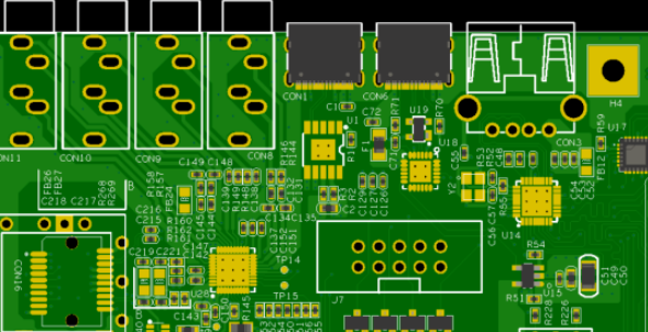
Another important aspect is the layer stack-up configuration.
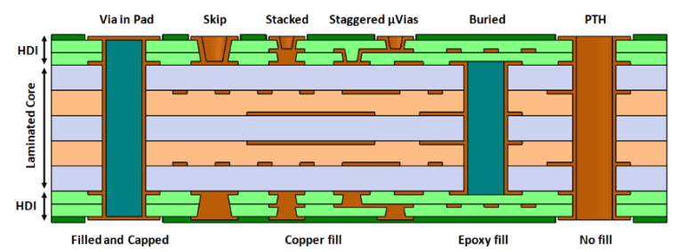
HDI PCBs typically feature multiple layers, including microvias, blind vias, and buried vias, which allow for greater routing density and more complex interconnections. The stack-up must be carefully designed to balance electrical performance with manufacturability. For instance, the use of sequential lamination processes can enable more intricate designs but may also increase production complexity and cost. Therefore, designers must weigh these factors to achieve an optimal balance.
Signal integrity is another critical consideration in HDI PCB layout.
As signal frequencies increase, issues such as impedance mismatches, reflections, and electromagnetic interference (EMI) become more pronounced. To mitigate these challenges, designers must employ techniques such as controlled impedance routing, differential pair routing, and the use of ground planes. These strategies help maintain signal integrity by minimizing disruptions and ensuring consistent signal paths.
Moreover, power integrity is equally important in HDI PCB design.
With the increasing power demands of modern electronic devices, ensuring stable power delivery is paramount. This involves careful planning of power distribution networks (PDNs) to minimize voltage drops and noise. Techniques such as the use of decoupling capacitors, power planes, and proper via placement can enhance power integrity by providing low-impedance paths for power delivery.
Thermal management is another crucial factor that cannot be overlooked.
As components become more densely packed, the risk of overheating increases, which can lead to performance degradation or even failure. Effective thermal management strategies, such as the use of thermal vias, heat sinks, and thermal interface materials, are essential to dissipate heat efficiently and maintain the reliability of the PCB.
Finally, manufacturability and cost considerations play a significant role in HDI PCB design. While advanced features such as finer lines and spaces, smaller vias, and more layers can enhance performance, they also increase manufacturing complexity and cost. Designers must collaborate closely with manufacturers to ensure that the design is not only functional but also feasible to produce within budget constraints.
In conclusion, the design of HDI PCBs involves a delicate balance of various factors, including material selection, layer stack-up, signal and power integrity, thermal management, and manufacturability. By carefully considering these aspects, designers can create HDI PCBs that meet the demanding requirements of modern electronic devices, ensuring both performance and reliability. As technology continues to evolve, staying informed about the latest advancements and best practices in HDI PCB design will be essential for success in this dynamic field.
Innovations In HDI PCB Manufacturing Techniques
High-Density Interconnect (HDI) printed circuit boards (PCBs) have become a cornerstone in the advancement of modern electronics, driven by the demand for more compact, efficient, and powerful devices. As technology continues to evolve, innovations in HDI PCB manufacturing techniques are playing a crucial role in meeting these demands. These innovations not only enhance the performance and reliability of electronic devices but also push the boundaries of what is possible in electronic design.
One of the most significant advancements in HDI PCB manufacturing is the development of laser drilling technology.
This technique allows for the creation of microvias, which are essential for the high-density interconnects that characterize HDI PCBs. Laser drilling offers precision and accuracy, enabling the production of smaller and more densely packed vias than traditional mechanical drilling methods. This precision is crucial for accommodating the increasing number of connections required in modern electronic devices, such as smartphones and tablets, without compromising on space or performance.
In addition to laser drilling, the use of advanced materials has also contributed to the evolution of HDI PCB manufacturing.
Materials such as high-performance laminates and copper foils are now being used to improve the thermal and electrical properties of PCBs. These materials not only enhance the durability and reliability of the boards but also allow for better heat dissipation, which is critical in preventing overheating in densely packed electronic components. As a result, devices can operate at higher speeds and with greater efficiency, meeting the ever-growing consumer expectations for performance.
Moreover, the integration of automated manufacturing processes has revolutionized the production of HDI PCBs.
Automation ensures consistency and precision in the manufacturing process, reducing the likelihood of human error and increasing production efficiency. This is particularly important in the context of HDI PCBs, where even minor deviations can lead to significant performance issues. Automated processes also facilitate the rapid prototyping and production of complex designs, allowing manufacturers to respond quickly to market demands and technological advancements.
Furthermore, the adoption of advanced design software has streamlined the HDI PCB design process.
These software tools enable designers to create intricate layouts with ease, optimizing the placement of components and interconnections to maximize performance and minimize space. The ability to simulate and test designs virtually before production reduces the risk of costly errors and accelerates the development cycle. This is particularly beneficial in industries such as consumer electronics and telecommunications, where time-to-market is a critical factor.
In conclusion, innovations in HDI PCB manufacturing techniques are driving the evolution of electronic devices, enabling them to become more compact, efficient, and powerful. The advancements in laser drilling, materials, automation, and design software are not only enhancing the capabilities of HDI PCBs but also setting new standards for performance and reliability. As technology continues to advance, it is likely that these innovations will further evolve, opening up new possibilities for electronic design and manufacturing. The ongoing development in this field underscores the importance of HDI PCBs in shaping the future of electronics, ensuring that they remain at the forefront of technological progress.
Challenges And Solutions In HDI PCB Design
High-Density Interconnect (HDI) printed circuit boards (PCBs) have become a cornerstone in the advancement of modern electronics, offering a pathway to more compact, efficient, and powerful devices. However, the design and implementation of HDI PCBs present a unique set of challenges that require innovative solutions. As the demand for smaller and more complex electronic devices continues to grow, engineers and designers must navigate these challenges to deliver high-performance products.
One of the primary challenges in HDI PCB design is managing the increased complexity that comes with higher component density.
As devices shrink in size, the need to fit more components into a limited space becomes paramount. This often results in intricate routing and the necessity for multiple layers within the PCB. To address this, designers employ advanced techniques such as microvias, blind and buried vias, and via-in-pad technology. These methods allow for more efficient use of space and enable the interconnection of densely packed components without compromising the board’s integrity.
Another significant challenge is signal integrity, which becomes increasingly critical as the density of the PCB increases.
High-speed signals are more susceptible to interference and crosstalk in densely packed environments. To mitigate these issues, designers must carefully consider the layout and routing of traces, ensuring that signal paths are optimized for minimal interference. Techniques such as differential signaling, controlled impedance routing, and the use of ground planes are essential in maintaining signal integrity. Additionally, simulation tools can be employed to predict and address potential signal integrity issues before the physical board is manufactured.
Thermal management is also a crucial consideration in HDI PCB design.
As more components are packed into a smaller area, the potential for heat buildup increases, which can adversely affect the performance and reliability of the device. Effective thermal management strategies are necessary to dissipate heat efficiently. This can be achieved through the use of thermal vias, heat sinks, and thermal interface materials. Moreover, careful placement of components and the strategic use of copper planes can help distribute heat more evenly across the board.
Manufacturability is another aspect that poses challenges in HDI PCB design.
The intricate nature of HDI boards requires precision manufacturing processes, which can be more costly and time-consuming than traditional PCB fabrication. To overcome these challenges, collaboration with experienced manufacturers is essential. Designers must ensure that their designs are not only functional but also manufacturable within the constraints of current technology. This often involves iterative design processes and close communication with manufacturing partners to refine designs for optimal production.
In conclusion, while HDI PCB design presents several challenges, the solutions available today enable designers to overcome these obstacles and create highly efficient and compact electronic devices. By leveraging advanced design techniques, maintaining a focus on signal integrity and thermal management, and collaborating closely with manufacturers, engineers can successfully navigate the complexities of HDI PCB design. As technology continues to evolve, ongoing innovation in design and manufacturing processes will be crucial in meeting the ever-increasing demands of the electronics industry.