Hdi pcb reliability
Factors Influencing HDI PCB Reliability
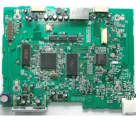
High-Density Interconnect (HDI) printed circuit boards (PCBs) have become a cornerstone in the advancement of modern electronics, offering enhanced performance and miniaturization capabilities. However, the reliability of HDI PCBs is a critical factor that determines their effectiveness in various applications, from consumer electronics to aerospace systems. Several factors influence the reliability of HDI PCBs, and understanding these can help in designing and manufacturing more robust and dependable boards.
To begin with, the choice of materials plays a pivotal role in the reliability of HDI PCBs.
The substrate material must possess excellent thermal and mechanical properties to withstand the stresses encountered during operation. Materials such as FR-4, polyimide, and ceramic are commonly used, each offering distinct advantages. For instance, FR-4 is widely used due to its cost-effectiveness and good thermal resistance, while polyimide offers superior flexibility and thermal stability, making it suitable for more demanding applications. The selection of the appropriate material is crucial, as it directly impacts the board’s ability to endure thermal cycling and mechanical stress.
In addition to material selection, the design of the HDI PCB significantly affects its reliability.
The layout must be meticulously planned to ensure optimal signal integrity and minimize electromagnetic interference. This involves careful consideration of trace widths, spacing, and the placement of vias. Microvias, a hallmark of HDI technology, allow for higher wiring density and improved electrical performance. However, their reliability is contingent upon proper design and manufacturing processes. Ensuring that microvias are correctly filled and plated is essential to prevent issues such as voids or cracks, which can lead to electrical failures.
Moreover, the manufacturing process itself is a critical determinant of HDI PCB reliability.
Advanced fabrication techniques, such as laser drilling and sequential lamination, are employed to achieve the high precision required for HDI boards. These processes must be meticulously controlled to prevent defects that could compromise the board’s performance. For example, laser drilling must be precisely calibrated to avoid damaging the substrate or creating irregular via walls. Similarly, the lamination process must ensure uniform pressure and temperature distribution to prevent delamination or warping.
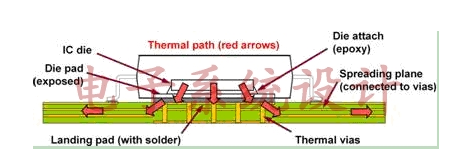
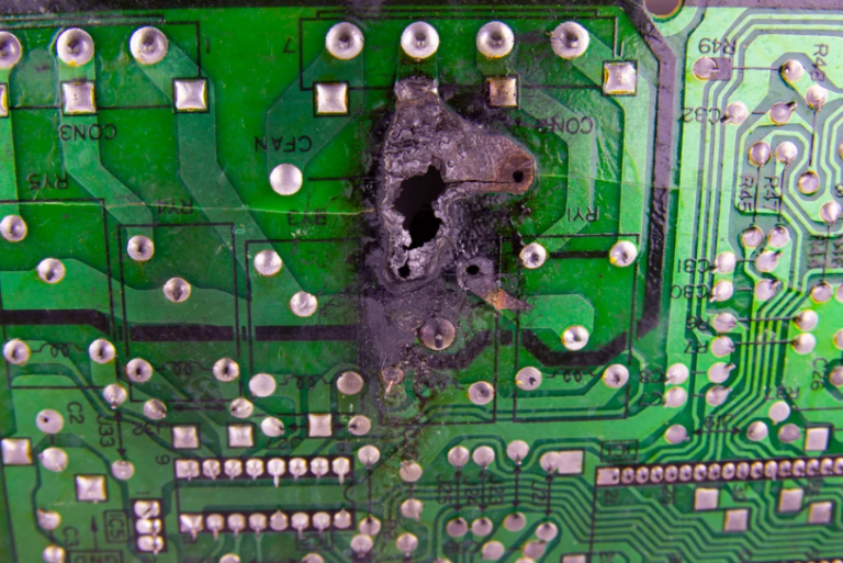
Thermal management is another crucial factor influencing the reliability of HDI PCBs.
As electronic devices become more compact and powerful, the heat generated during operation can pose significant challenges. Effective thermal management strategies, such as the use of thermal vias, heat sinks, and conductive materials, are essential to dissipate heat and maintain the board’s performance. Failure to adequately manage heat can lead to thermal stress, which may cause material degradation and ultimately result in board failure.
Furthermore, environmental factors such as humidity, temperature fluctuations, and exposure to corrosive elements can impact the reliability of HDI PCBs.
Protective coatings, such as conformal coatings or encapsulants, are often applied to shield the board from these environmental stresses. These coatings must be carefully selected and applied to ensure they provide adequate protection without interfering with the board’s electrical performance.
In conclusion, the reliability of HDI PCBs is influenced by a multitude of factors, including material selection, design considerations, manufacturing processes, thermal management, and environmental protection. By addressing these factors comprehensively, manufacturers can enhance the reliability of HDI PCBs, ensuring their performance and longevity in a wide range of applications. As technology continues to evolve, ongoing research and development in these areas will be essential to meet the increasing demands for reliable and high-performance electronic devices.
Design Best Practices for Enhancing HDI PCB Reliability
In the realm of modern electronics, High-Density Interconnect (HDI) printed circuit boards (PCBs) have emerged as a pivotal technology, enabling the miniaturization and enhanced performance of electronic devices. As the demand for compact and efficient devices continues to rise, ensuring the reliability of HDI PCBs becomes paramount. To achieve this, adopting design best practices is essential, as it not only enhances the performance but also extends the lifespan of these intricate components.
To begin with, one of the fundamental aspects of enhancing HDI PCB reliability is the meticulous selection of materials.
The choice of substrate material significantly influences the board’s thermal and mechanical properties. High-quality materials with low coefficients of thermal expansion (CTE) are preferred, as they minimize the risk of delamination and mechanical stress during thermal cycling. Furthermore, selecting materials with superior dielectric properties ensures signal integrity, which is crucial for high-speed applications.
Transitioning to the design phase, implementing a robust layer stack-up is critical.
A well-planned stack-up not only optimizes the electrical performance but also enhances the board’s structural integrity. By strategically arranging power and ground planes, designers can reduce electromagnetic interference (EMI) and improve signal integrity. Additionally, maintaining symmetry in the stack-up helps in minimizing warpage, which is a common issue in HDI PCBs due to their complex structures.
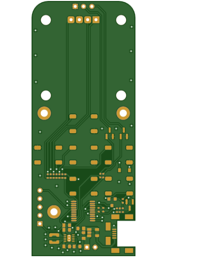
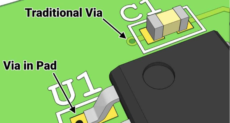
Another vital consideration is the via design, which plays a crucial role in the reliability of HDI PCBs.
Microvias, a hallmark of HDI technology, must be designed with precision to ensure mechanical stability and electrical performance. It is advisable to limit the aspect ratio of microvias to prevent issues such as plating voids and cracks. Moreover, employing staggered or stacked via configurations can enhance routing density while maintaining reliability. Careful attention to via-in-pad designs can also mitigate solderability issues and improve thermal management.
In addition to via design, trace routing demands careful consideration.
As HDI PCBs often accommodate high-speed signals, maintaining controlled impedance is essential. Designers should adhere to best practices such as using differential pairs and maintaining consistent trace widths and spacing. Furthermore, minimizing the length of signal paths and avoiding sharp angles can reduce signal reflections and losses, thereby enhancing overall performance.
Thermal management is another critical aspect that cannot be overlooked.
As electronic devices become more powerful, effective heat dissipation becomes increasingly important. Incorporating thermal vias, heat sinks, and thermal pads can significantly improve heat distribution across the board. Additionally, selecting materials with high thermal conductivity and designing for optimal airflow can further enhance thermal performance.
Finally, rigorous testing and validation are indispensable in ensuring HDI PCB reliability.
Conducting comprehensive simulations and stress tests can identify potential failure points and allow for design adjustments before mass production. Employing techniques such as accelerated life testing and thermal cycling can provide valuable insights into the board’s long-term performance under various conditions.
In conclusion, enhancing the reliability of HDI PCBs requires a holistic approach that encompasses material selection, design optimization, and thorough testing. By adhering to these best practices, designers can create robust and reliable HDI PCBs that meet the demands of modern electronic applications. As technology continues to evolve, the importance of reliable HDI PCBs will only grow, underscoring the need for continued innovation and adherence to design excellence.

Material Selection and Its Impact on HDI PCB Reliability
In the realm of electronics manufacturing, the reliability of High-Density Interconnect (HDI) printed circuit boards (PCBs) is of paramount importance. As devices become increasingly compact and complex, the demand for HDI PCBs has surged, necessitating a closer examination of the factors that influence their reliability. Among these factors, material selection plays a crucial role, impacting not only the performance but also the longevity of the PCBs. Understanding the interplay between material properties and HDI PCB reliability is essential for manufacturers aiming to produce durable and efficient electronic components.
To begin with, the choice of substrate material is a fundamental consideration in HDI PCB design.
The substrate serves as the foundation upon which the entire circuit is built, and its properties significantly affect the board’s thermal and mechanical performance. Commonly used materials include FR-4, a glass-reinforced epoxy laminate, and more advanced options like polyimide and ceramic substrates. FR-4 is favored for its cost-effectiveness and adequate performance in many applications. However, for high-frequency or high-temperature environments, polyimide and ceramic substrates offer superior thermal stability and electrical insulation, thereby enhancing the reliability of the HDI PCB.
In addition to the substrate, the selection of conductive materials is equally critical.
Copper is the predominant choice for conductive traces due to its excellent electrical conductivity and relatively low cost. However, the thickness and purity of the copper layer can influence the board’s performance. Thicker copper layers can handle higher current loads, reducing the risk of overheating and potential failure. Moreover, the use of high-purity copper minimizes the risk of corrosion and electromigration, both of which can compromise the integrity of the circuit over time.
Furthermore, the choice of dielectric materials, which insulate the conductive layers from each other, also impacts HDI PCB reliability.
Dielectric materials must possess low dielectric constant and loss tangent values to ensure signal integrity, especially in high-frequency applications. Materials such as PTFE (polytetrafluoroethylene) and certain advanced ceramics are often employed for their superior dielectric properties. These materials help maintain signal clarity and reduce the risk of crosstalk, thereby enhancing the overall reliability of the HDI PCB.
Moreover, the solder mask, which protects the copper traces from environmental factors and prevents solder bridging during assembly, is another critical material consideration.
The solder mask must be carefully selected to withstand the thermal cycles and chemical exposures typical in the operating environment of the PCB. High-quality solder masks can prevent moisture ingress and chemical corrosion, both of which can lead to premature failure of the board.
In conclusion, the reliability of HDI PCBs is intricately linked to the materials chosen during the design and manufacturing process. Each material, from the substrate to the solder mask, plays a vital role in determining the board’s ability to perform under various conditions. By carefully selecting materials that align with the specific requirements of the application, manufacturers can significantly enhance the reliability and longevity of HDI PCBs. As technology continues to advance, ongoing research and development in material science will undoubtedly lead to even more robust solutions, further solidifying the role of material selection in ensuring HDI PCB reliability.
Testing and Quality Assurance for HDI PCB Reliability
High-Density Interconnect (HDI) printed circuit boards (PCBs) have become a cornerstone in the advancement of modern electronics, offering enhanced performance and miniaturization capabilities. As these PCBs are integral to critical applications, ensuring their reliability through rigorous testing and quality assurance processes is paramount. The reliability of HDI PCBs is contingent upon a comprehensive understanding of their unique characteristics and the implementation of meticulous testing protocols.
To begin with, HDI PCBs are distinguished by their finer lines and spaces, smaller vias, and higher connection pad density.
These features, while advantageous for compact and complex designs, also introduce potential reliability challenges. Therefore, testing and quality assurance must be tailored to address these specific attributes. One of the primary testing methods employed is thermal cycling, which evaluates the board’s ability to withstand temperature fluctuations. This is crucial because HDI PCBs are often used in environments where they are subjected to varying thermal conditions. By simulating these conditions, manufacturers can identify potential failure points, such as delamination or via cracking, which could compromise the board’s functionality.
In addition to thermal cycling, electrical testing is another critical component of the quality assurance process.
This involves checking for continuity and isolation to ensure that the electrical pathways are intact and that there are no unintended connections. Given the intricate nature of HDI PCBs, even minor defects can lead to significant performance issues. Therefore, advanced testing techniques, such as automated optical inspection (AOI) and X-ray inspection, are employed to detect defects that may not be visible to the naked eye. These methods allow for a non-destructive evaluation of the board, ensuring that any potential issues are identified and rectified before the product reaches the end user.
Moreover, the reliability of HDI PCBs is also influenced by the materials used in their construction.
High-quality materials that can withstand environmental stresses are essential for ensuring long-term reliability. Consequently, material testing is an integral part of the quality assurance process. This includes assessing the thermal and mechanical properties of the substrate materials, as well as the adhesion strength of the copper layers. By ensuring that the materials meet stringent standards, manufacturers can enhance the durability and performance of the final product.
Furthermore, process control is a vital aspect of ensuring HDI PCB reliability.
This involves monitoring and controlling the various stages of the manufacturing process to prevent defects from occurring. Statistical process control (SPC) techniques are often employed to maintain consistency and quality throughout production. By analyzing data from the manufacturing process, potential issues can be identified and addressed proactively, reducing the likelihood of defects in the final product.
In conclusion, the reliability of HDI PCBs is a multifaceted issue that requires a comprehensive approach to testing and quality assurance.
By employing a combination of thermal, electrical, and material testing, along with stringent process control measures, manufacturers can ensure that their products meet the high standards required for modern electronic applications. As technology continues to evolve, the importance of reliable HDI PCBs will only increase, making these testing and quality assurance processes more critical than ever. Through continuous improvement and innovation in testing methodologies, the industry can continue to deliver reliable and high-performing HDI PCBs that meet the demands of today’s technology-driven world.