Hdi pcb reliability
Factors Influencing HDI PCB Reliability
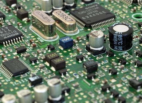
High-Density Interconnect (HDI) printed circuit boards (PCBs) have become a cornerstone in the advancement of modern electronics, offering enhanced performance and miniaturization capabilities.
However, the reliability of HDI PCBs is influenced by a multitude of factors that must be meticulously considered during the design and manufacturing processes.
Understanding these factors is crucial for ensuring the longevity and functionality of electronic devices that rely on HDI technology.
One of the primary factors affecting HDI PCB reliability is the choice of materials.
The materials used in the fabrication of HDI PCBs must possess excellent thermal and mechanical properties to withstand the stresses encountered during operation. For instance, the dielectric materials should have a low coefficient of thermal expansion (CTE) to minimize the risk of delamination and cracking under thermal cycling. Additionally, the copper used for traces and vias must exhibit high conductivity and adhesion to ensure efficient signal transmission and mechanical stability.
Moreover, the design of the HDI PCB plays a significant role in its reliability.
The layout must be optimized to reduce electromagnetic interference (EMI) and signal integrity issues, which can degrade performance over time. This involves careful consideration of trace width, spacing, and the placement of components to minimize crosstalk and impedance mismatches. Furthermore, the use of blind and buried vias, a hallmark of HDI technology, requires precise drilling and plating techniques to maintain electrical connectivity and structural integrity.
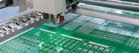
Transitioning to the manufacturing process, the precision and quality control measures employed during production are critical to HDI PCB reliability.
Advanced fabrication techniques, such as laser drilling and sequential lamination, must be executed with high accuracy to ensure the proper formation of microvias and multilayer structures. Any deviation from specified parameters can lead to defects such as voids, misalignments, or incomplete connections, which can compromise the board’s performance and durability.
In addition to manufacturing precision, environmental factors also influence HDI PCB reliability.
Exposure to extreme temperatures, humidity, and corrosive environments can accelerate the degradation of materials and solder joints. Therefore, it is essential to conduct thorough environmental testing and implement protective measures, such as conformal coatings, to shield the PCB from adverse conditions. These protective layers can prevent moisture ingress and reduce the risk of corrosion, thereby extending the lifespan of the board.
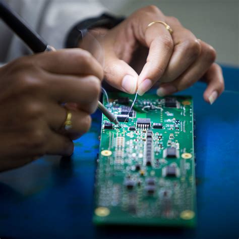
Furthermore, the reliability of HDI PCBs is contingent upon the quality of assembly processes.
The soldering techniques used to attach components to the board must ensure robust mechanical and electrical connections. This involves selecting appropriate solder alloys and fluxes, as well as optimizing reflow profiles to prevent defects such as solder voids and bridging. Additionally, the use of automated optical inspection (AOI) and X-ray inspection can help identify and rectify assembly defects before the final product is deployed.
In conclusion, the reliability of HDI PCBs is a multifaceted issue that hinges on material selection, design optimization, manufacturing precision, environmental protection, and assembly quality. By addressing these factors comprehensively, manufacturers can enhance the performance and durability of HDI PCBs, thereby meeting the stringent demands of modern electronic applications. As technology continues to evolve, ongoing research and development in these areas will be essential to further improve the reliability of HDI PCBs and support the next generation of electronic innovations.
Design Best Practices for Enhancing HDI PCB Reliability
High-Density Interconnect (HDI) printed circuit boards (PCBs) have become a cornerstone in modern electronics, offering enhanced performance and miniaturization capabilities. As devices become increasingly compact and complex, the reliability of HDI PCBs is paramount. To ensure optimal performance and longevity, designers must adhere to best practices that enhance the reliability of these intricate boards.
One of the primary considerations in HDI PCB design is the selection of materials.
The choice of substrate material significantly impacts the board’s thermal and mechanical properties. High-quality materials with low coefficients of thermal expansion (CTE) are preferred, as they minimize the risk of delamination and warping under thermal stress. Additionally, using materials with high glass transition temperatures (Tg) ensures that the board can withstand higher operating temperatures without degradation.
Transitioning from material selection to design layout, the importance of via design cannot be overstated.
Microvias, a hallmark of HDI technology, must be carefully designed to maintain structural integrity. Ensuring that microvias are properly filled and plated is crucial to prevent voids and ensure reliable electrical connections. Moreover, staggering microvias rather than stacking them can enhance mechanical strength and reduce the risk of failure.
Another critical aspect of HDI PCB design is the management of signal integrity.
As the density of interconnections increases, so does the potential for signal interference. To mitigate this, designers should employ techniques such as controlled impedance routing and differential pair routing. These methods help maintain signal integrity by minimizing crosstalk and electromagnetic interference. Furthermore, incorporating adequate ground planes and shielding can further enhance signal reliability.
Thermal management is another vital consideration in HDI PCB design.
As electronic components become more densely packed, effective heat dissipation becomes challenging yet essential. Designers should incorporate thermal vias and heat sinks to facilitate efficient heat transfer away from critical components. Additionally, using thermal simulation tools during the design phase can help identify potential hotspots and optimize the thermal performance of the board.
Transitioning to the manufacturing process, ensuring precision and accuracy is crucial for HDI PCB reliability.
Advanced fabrication techniques, such as laser drilling and sequential lamination, are often employed to achieve the fine features required by HDI designs. It is essential to work closely with experienced manufacturers who understand the intricacies of HDI technology and can maintain tight tolerances throughout the production process.
Finally, rigorous testing and quality assurance are indispensable in verifying the reliability of HDI PCBs. Implementing comprehensive testing protocols, including electrical testing, thermal cycling, and mechanical stress testing, can identify potential weaknesses before the boards are deployed in the field. Additionally, employing design for testability (DFT) principles during the design phase can facilitate easier testing and troubleshooting.
In conclusion, enhancing the reliability of HDI PCBs requires a holistic approach that encompasses material selection, design layout, signal integrity management, thermal management, precise manufacturing, and thorough testing. By adhering to these best practices, designers can ensure that their HDI PCBs meet the demanding requirements of modern electronic applications, providing robust performance and longevity in increasingly compact and complex devices.
Material Selection and Its Impact on HDI PCB Reliability
In the realm of electronics manufacturing, the reliability of High-Density Interconnect (HDI) printed circuit boards (PCBs) is of paramount importance. As devices become increasingly compact and complex, the demand for HDI PCBs has surged, necessitating a closer examination of the factors that influence their reliability.
Among these factors, material selection plays a crucial role, impacting not only the performance but also the longevity of the PCBs. Understanding the interplay between material properties and HDI PCB reliability is essential for manufacturers aiming to produce durable and efficient electronic components.
To begin with, the choice of substrate material is a fundamental consideration in HDI PCB design.
The substrate serves as the foundation of the PCB, providing mechanical support and electrical insulation. Common materials include FR-4, a glass-reinforced epoxy laminate, and more advanced options like polyimide and ceramic substrates. Each material offers distinct advantages and limitations. For instance, FR-4 is widely used due to its cost-effectiveness and satisfactory performance in many applications. However, for high-frequency or high-temperature environments, polyimide or ceramic substrates may be preferred due to their superior thermal stability and dielectric properties. Consequently, selecting the appropriate substrate material is critical to ensuring the HDI PCB can withstand the operational stresses it will encounter.
In addition to the substrate, the choice of conductive materials significantly affects HDI PCB reliability.
Copper is the predominant choice for conductive traces due to its excellent electrical conductivity and thermal performance. However, the thickness and quality of the copper layer must be carefully controlled. Thinner copper layers, while beneficial for achieving finer traces and spaces, may be more susceptible to issues such as electromigration and thermal fatigue. Therefore, a balance must be struck between achieving the desired electrical performance and maintaining structural integrity. Furthermore, surface finishes applied to copper traces, such as immersion gold or organic solderability preservatives, can influence the board’s resistance to oxidation and corrosion, thereby impacting long-term reliability.
Moreover, the dielectric materials used in HDI PCBs also play a pivotal role in determining their reliability.
Dielectrics are essential for insulating conductive layers and maintaining signal integrity. The dielectric constant and loss tangent of these materials must be carefully considered, as they affect signal speed and attenuation. Low-loss dielectrics are often preferred for high-frequency applications to minimize signal degradation. Additionally, the thermal properties of dielectric materials, such as their glass transition temperature and coefficient of thermal expansion, must align with the overall thermal management strategy of the PCB to prevent delamination and mechanical failure.
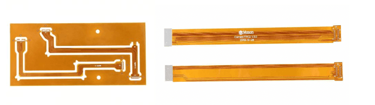
Furthermore, the integration of microvias, a hallmark of HDI technology, introduces additional material considerations.
The reliability of microvias is heavily dependent on the materials used for their formation and filling. Laser-drilled microvias require precise control over the dielectric material to ensure clean and reliable connections. The choice of via fill material, whether conductive or non-conductive, also impacts the mechanical and thermal performance of the PCB. Proper material selection and process control are essential to prevent common issues such as via cracking and void formation.
In conclusion, the reliability of HDI PCBs is intricately linked to the materials chosen during their design and manufacturing processes. From substrates and conductive layers to dielectrics and microvias, each material component must be carefully evaluated to ensure it meets the specific demands of the application. By understanding the material properties and their interactions, manufacturers can enhance the reliability and performance of HDI PCBs, ultimately contributing to the success of the electronic devices they support.
Testing and Quality Assurance for Reliable HDI PCBs
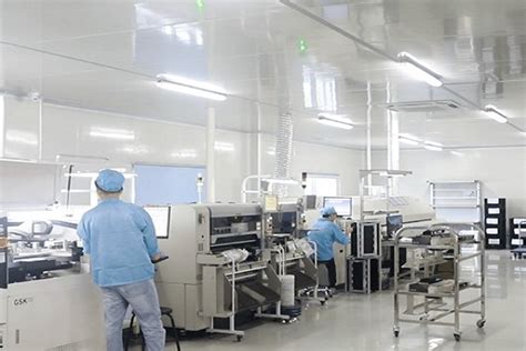
In the realm of modern electronics, High-Density Interconnect (HDI) printed circuit boards (PCBs) have emerged as a pivotal component, enabling the miniaturization and enhanced performance of electronic devices. As the demand for more compact and efficient devices continues to rise, ensuring the reliability of HDI PCBs becomes paramount. This necessitates rigorous testing and quality assurance processes to guarantee that these intricate boards meet the high standards required for their diverse applications.
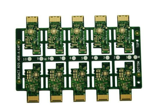
To begin with, the complexity of HDI PCBs, characterized by their fine lines, microvias, and multiple layers, presents unique challenges in testing and quality assurance.
The intricate design of these boards requires advanced testing methodologies to detect potential defects that could compromise their functionality. One of the primary testing techniques employed is Automated Optical Inspection (AOI), which utilizes high-resolution cameras to scrutinize the board for any visual defects such as misalignments, open circuits, or soldering issues. AOI serves as a crucial first step in the quality assurance process, allowing for the early detection of defects that could lead to failures in the field.
In addition to AOI, electrical testing is indispensable in assessing the reliability of HDI PCBs.
This involves subjecting the boards to a series of electrical tests to verify the integrity of the circuits and ensure that they meet the specified electrical parameters. Flying probe testing, for instance, is a non-contact method that uses moving probes to test the electrical performance of the board without the need for a physical test fixture. This method is particularly advantageous for HDI PCBs due to its flexibility and ability to accommodate the complex designs typical of these boards.
Moreover, environmental testing plays a critical role in evaluating the durability of HDI PCBs under various conditions.
These tests simulate the environmental stresses that the boards may encounter during their operational life, such as temperature fluctuations, humidity, and mechanical vibrations. Thermal cycling tests, for example, expose the boards to extreme temperature variations to assess their ability to withstand thermal stress without failure. Such tests are essential in ensuring that HDI PCBs can maintain their performance and reliability in diverse and challenging environments.
Furthermore, the implementation of stringent quality assurance protocols is vital in the production of reliable HDI PCBs.
This involves establishing comprehensive quality control measures throughout the manufacturing process, from the selection of raw materials to the final inspection of the finished product. Statistical process control (SPC) techniques are often employed to monitor and control the manufacturing process, ensuring that any deviations from the desired specifications are promptly identified and corrected. By maintaining a high level of quality control, manufacturers can significantly reduce the likelihood of defects and enhance the overall reliability of the HDI PCBs.
In conclusion, the reliability of HDI PCBs is contingent upon a robust framework of testing and quality assurance practices.
Through the integration of advanced testing techniques such as AOI and flying probe testing, along with rigorous environmental assessments and quality control measures, manufacturers can ensure that these sophisticated boards meet the demanding requirements of modern electronic applications. As technology continues to evolve, the importance of reliable HDI PCBs will only grow, underscoring the need for ongoing advancements in testing and quality assurance methodologies to keep pace with the ever-increasing complexity of electronic devices.