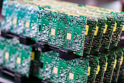
Hdi pcb structure
Understanding the Layers: A Deep Dive into HDI PCB Structure
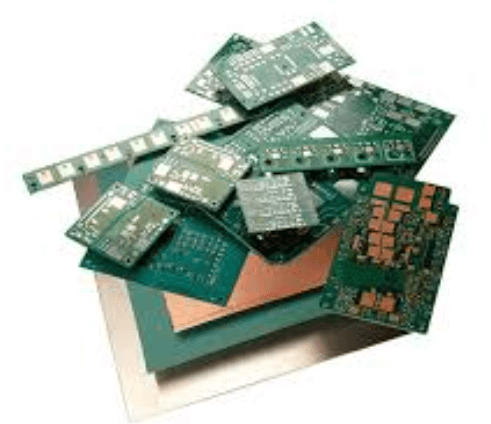
High-Density Interconnect (HDI) printed circuit boards (PCBs) represent a significant advancement in the field of electronics, offering enhanced performance and miniaturization capabilities.
Understanding the structure of HDI PCBs is crucial for appreciating their role in modern electronic devices.
At the core of HDI technology is the ability to incorporate more components in a smaller area, which is achieved through a sophisticated layering process. This process involves multiple layers of copper and insulating material, intricately designed to optimize space and functionality.
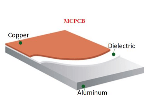
The foundation of an HDI PCB is its substrate, typically made from materials like FR-4, which provides mechanical support and electrical insulation.
This substrate serves as the base upon which the intricate network of copper traces and vias are built. The copper layers are essential for conducting electrical signals across the board, and in HDI PCBs, these layers are often thinner and more densely packed than in traditional PCBs. This density is achieved through the use of microvias, which are small holes that connect different layers of the board. Unlike traditional vias, microvias are much smaller and can be placed more closely together, allowing for a higher density of connections.
Transitioning from the substrate, the next critical component in HDI PCB structure is the dielectric material.
This insulating layer separates the copper layers, preventing electrical interference and ensuring signal integrity. The choice of dielectric material is crucial, as it affects the board’s thermal and electrical properties. Advanced materials with low dielectric constants are often used to enhance signal speed and reduce power loss. Furthermore, the dielectric layers in HDI PCBs are typically thinner than those in conventional PCBs, contributing to the overall compactness of the board.
As we delve deeper into the structure, it becomes evident that the arrangement of layers in an HDI PCB is not arbitrary.
The stack-up configuration, which refers to the order and number of layers, is meticulously designed to meet specific performance requirements. For instance, a common stack-up might include multiple signal layers, power and ground planes, and additional layers for shielding and heat dissipation. This configuration allows for efficient routing of signals and power distribution, which is essential for high-speed and high-frequency applications.
Moreover, the use of blind and buried vias further enhances the complexity and capability of HDI PCBs.
Blind vias connect an outer layer to one or more inner layers without passing through the entire board, while buried vias connect only internal layers. These types of vias enable more routing options and contribute to the board’s compact design. The integration of these features allows HDI PCBs to support advanced functionalities in a wide range of applications, from smartphones and tablets to aerospace and medical devices.
In conclusion, the structure of HDI PCBs is a testament to the advancements in electronic design and manufacturing. By leveraging multiple layers, microvias, and advanced materials, HDI PCBs achieve a level of miniaturization and performance that is essential for modern technology. Understanding the intricacies of their structure provides insight into how these boards support the ever-increasing demands for smaller, faster, and more efficient electronic devices. As technology continues to evolve, the role of HDI PCBs will undoubtedly expand, driving further innovation in the electronics industry.
The Role of Microvias in HDI PCB Design
High-Density Interconnect (HDI) printed circuit boards (PCBs) have become a cornerstone in the advancement of modern electronics, primarily due to their ability to accommodate complex circuitry within a compact space. A critical component in the design and functionality of HDI PCBs is the microvia, which plays a pivotal role in enhancing the performance and reliability of these sophisticated boards. Understanding the role of microvias in HDI PCB design requires an exploration of their structure, benefits, and the technological advancements they enable.
Microvias are small-diameter vias, typically less than 150 micrometers, that connect different layers of a PCB.
Unlike traditional vias, which can extend through the entire board, microvias are often used in a staggered or stacked configuration to connect only adjacent layers. This characteristic allows for a significant reduction in the space required for interconnections, thereby enabling the design of more compact and efficient PCBs. The ability to place components closer together without compromising connectivity is a fundamental advantage of microvias, facilitating the miniaturization of electronic devices.
The implementation of microvias in HDI PCBs offers several benefits that are crucial for modern electronic applications.
Firstly, microvias contribute to improved electrical performance by reducing the inductance and capacitance associated with longer interconnections. This reduction is particularly beneficial in high-frequency applications, where signal integrity is paramount. Additionally, the shorter path lengths provided by microvias help minimize signal loss and electromagnetic interference, further enhancing the overall performance of the PCB.
Moreover, microvias enable increased routing density, which is essential for accommodating the growing complexity of electronic circuits.
As devices become more sophisticated, the demand for additional functionality within a limited space intensifies. Microvias address this challenge by allowing designers to incorporate more layers and finer traces without increasing the board’s overall size. This capability is particularly advantageous in applications such as smartphones, tablets, and wearable technology, where space is at a premium.
The use of microvias also contributes to improved thermal management within HDI PCBs.
By facilitating efficient heat dissipation through the board, microvias help prevent overheating, which can lead to component failure and reduced reliability. This aspect is especially important in high-power applications, where effective thermal management is critical to maintaining optimal performance and extending the lifespan of the device.
In addition to these benefits, the integration of microvias in HDI PCB design supports the trend towards more environmentally friendly manufacturing processes.
The reduced material usage and smaller board sizes associated with microvias contribute to a decrease in waste and resource consumption. Furthermore, advancements in laser drilling technology have made the production of microvias more precise and efficient, reducing the environmental impact of PCB manufacturing.
In conclusion, microvias are an indispensable element in the design of HDI PCBs, offering numerous advantages that align with the demands of modern electronic devices. Their ability to enhance electrical performance, increase routing density, improve thermal management, and support sustainable manufacturing practices underscores their significance in the evolution of PCB technology. As electronic devices continue to evolve, the role of microvias in HDI PCB design will undoubtedly remain a critical factor in meeting the challenges of miniaturization and performance optimization.
Comparing HDI PCB Structure with Traditional PCB Designs
High-Density Interconnect (HDI) printed circuit boards (PCBs) represent a significant advancement in the field of electronics, offering a stark contrast to traditional PCB designs. As technology continues to evolve, the demand for more compact, efficient, and high-performing electronic devices has driven the development of HDI PCBs. To understand the differences between HDI and traditional PCBs, it is essential to examine their structures, capabilities, and applications.
Traditional PCBs typically consist of a few layers, with through-hole technology being the primary method for connecting components.
These boards are generally sufficient for less complex electronic devices, where space and performance are not critical constraints. However, as electronic devices have become more sophisticated, the limitations of traditional PCBs have become apparent. The need for increased functionality, reduced size, and enhanced performance has led to the development of HDI PCBs, which offer a more advanced structural design.
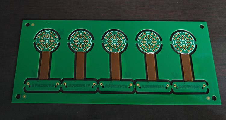
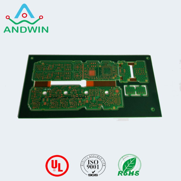
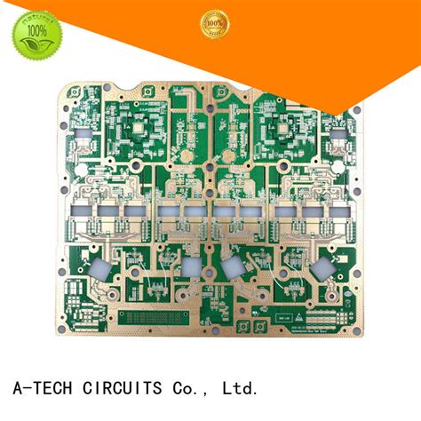
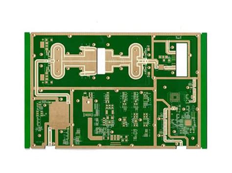
HDI PCBs are characterized by their use of microvias, blind vias, and buried vias, which allow for a higher density of interconnections.
This structural innovation enables the placement of more components in a smaller area, significantly reducing the overall size of the PCB. The use of microvias, in particular, is a defining feature of HDI PCBs. These small-diameter vias allow for connections between layers without occupying excessive space, thus facilitating the design of more compact and efficient circuits.
In addition to their compact size, HDI PCBs offer improved electrical performance.
The shorter distances between components reduce signal loss and improve signal integrity, which is crucial for high-speed applications. This is particularly important in modern electronics, where data transfer rates and processing speeds are continually increasing. The enhanced electrical performance of HDI PCBs makes them ideal for use in advanced applications such as smartphones, tablets, and other portable devices, where space is at a premium and performance cannot be compromised.
Moreover, the manufacturing process of HDI PCBs differs from that of traditional PCBs, incorporating advanced techniques such as laser drilling and sequential lamination.
These processes allow for the precise creation of microvias and the integration of multiple layers, contributing to the overall efficiency and reliability of the board. While the manufacturing of HDI PCBs can be more complex and costly compared to traditional methods, the benefits they offer in terms of performance and miniaturization often justify the investment.
Furthermore, the versatility of HDI PCBs extends beyond consumer electronics.
They are increasingly being used in automotive, aerospace, and medical applications, where reliability and performance are critical. The ability to integrate more functionality into a smaller footprint makes HDI PCBs an attractive option for these industries, where space constraints and high-performance requirements are common challenges.
In conclusion, the structural differences between HDI and traditional PCBs highlight the advancements in PCB technology driven by the demands of modern electronics. HDI PCBs offer a compact, high-performance solution that meets the needs of today’s complex electronic devices. As technology continues to advance, the role of HDI PCBs is likely to expand, further bridging the gap between traditional designs and the future of electronic innovation.
Innovations in HDI PCB Structure for Enhanced Performance
High-Density Interconnect (HDI) printed circuit boards (PCBs) have become a cornerstone in the advancement of modern electronics, offering a compact and efficient solution for increasingly complex electronic designs. As the demand for smaller, faster, and more efficient devices continues to grow, innovations in HDI PCB structure are pivotal in meeting these requirements. These innovations not only enhance the performance of electronic devices but also push the boundaries of what is technologically possible.
To begin with, HDI PCBs are characterized by their higher wiring density per unit area compared to traditional PCBs.
This is achieved through the use of finer lines and spaces, smaller vias, and capture pads, as well as higher connection pad density. The miniaturization of these components allows for more functionality to be packed into a smaller space, which is essential for modern electronic devices such as smartphones, tablets, and wearable technology. The ability to incorporate more components into a smaller area without compromising performance is a significant advantage of HDI technology.
One of the key innovations in HDI PCB structure is the use of microvias, which are significantly smaller than traditional vias.
Microvias allow for more interconnections in a given area, thereby increasing the routing density. This is particularly beneficial in multilayer PCBs, where space is at a premium. The use of microvias not only saves space but also reduces the inductance and capacitance of the circuit, leading to improved signal integrity and faster signal transmission. Consequently, devices can operate at higher speeds with greater efficiency.
Moreover, the incorporation of advanced materials in HDI PCBs has further enhanced their performance.
For instance, the use of low-loss materials helps in reducing signal loss, which is crucial for high-frequency applications. These materials also offer better thermal management, which is essential for maintaining the reliability and longevity of electronic devices. As electronic devices become more powerful, effective heat dissipation becomes increasingly important to prevent overheating and ensure stable operation.
In addition to material advancements, the adoption of laser drilling technology has revolutionized the manufacturing process of HDI PCBs.
Laser drilling allows for the precise creation of microvias, which is essential for maintaining the integrity of the circuit. This technology not only improves the accuracy and reliability of the manufacturing process but also reduces production time and costs. As a result, manufacturers can produce high-quality HDI PCBs more efficiently, making them more accessible for a wide range of applications.
Furthermore, the integration of embedded components within HDI PCBs represents another significant innovation.
By embedding passive components such as resistors and capacitors within the layers of the PCB, designers can save space on the surface of the board. This not only contributes to the miniaturization of electronic devices but also enhances their performance by reducing parasitic effects and improving electrical characteristics.
In conclusion, the continuous innovations in HDI PCB structure are instrumental in advancing the capabilities of modern electronic devices. Through the use of microvias, advanced materials, laser drilling technology, and embedded components, HDI PCBs offer enhanced performance, greater efficiency, and increased functionality. As technology continues to evolve, the role of HDI PCBs in shaping the future of electronics remains indispensable, driving the development of smaller, faster, and more powerful devices.