Heavy copper board for pcb
Advantages Of Using Heavy Copper Boards In PCB Design
In the realm of printed circuit board (PCB) design, the choice of materials and components plays a crucial role in determining the performance and reliability of the final product. Among the various options available, heavy copper boards have emerged as a significant innovation, offering a range of advantages that make them an attractive choice for many applications. As we delve into the benefits of using heavy copper boards in PCB design, it becomes evident that their unique properties can address several challenges faced by engineers and designers.
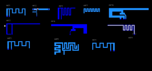
To begin with, heavy copper boards are characterized by their thicker copper layers, typically exceeding three ounces per square foot.
This increased thickness provides a substantial improvement in current-carrying capacity, which is particularly beneficial for high-power applications. In scenarios where standard PCBs might struggle to handle large currents without overheating, heavy copper boards excel by efficiently distributing heat and minimizing the risk of thermal failure. Consequently, this makes them ideal for power electronics, automotive systems, and industrial applications where reliability is paramount.
Moreover, the enhanced thermal management capabilities of heavy copper boards extend beyond mere current handling.
The thicker copper layers facilitate superior heat dissipation, which is crucial for maintaining optimal operating temperatures in high-performance devices. By effectively managing heat, these boards help prevent component degradation and extend the lifespan of the entire system. This is especially important in environments where temperature fluctuations are common, as heavy copper boards can maintain stability and performance under varying conditions.
In addition to thermal advantages, heavy copper boards offer improved mechanical strength and durability.
The robust construction of these boards makes them resistant to mechanical stresses, such as bending and vibration, which can be detrimental to standard PCBs. This increased resilience ensures that heavy copper boards can withstand harsh operating conditions, making them suitable for use in aerospace, military, and other demanding industries. Furthermore, their durability translates to a longer service life, reducing the need for frequent replacements and maintenance.
Another noteworthy advantage of heavy copper boards is their ability to support complex and compact designs.
The increased copper thickness allows for the integration of multiple layers and intricate circuit patterns without compromising performance. This capability is particularly advantageous in modern electronic devices, where space is often at a premium. By enabling more compact designs, heavy copper boards contribute to the miniaturization of technology, facilitating the development of smaller, more efficient products.
Furthermore, the use of heavy copper boards can lead to cost savings in the long run.
Although the initial manufacturing costs may be higher compared to standard PCBs, the enhanced performance, reliability, and longevity of heavy copper boards can result in reduced operational and maintenance expenses. This cost-effectiveness is a compelling factor for industries seeking to optimize their production processes and achieve a favorable return on investment.
In conclusion, the advantages of using heavy copper boards in PCB design are manifold, encompassing improved current-carrying capacity, superior thermal management, enhanced mechanical strength, support for complex designs, and potential cost savings. As technology continues to advance and the demand for high-performance electronic devices grows, heavy copper boards are poised to play an increasingly vital role in meeting these challenges. By leveraging their unique properties, engineers and designers can create more reliable, efficient, and durable products, ultimately driving innovation across various sectors.
Manufacturing Techniques For Heavy Copper PCBs
In the realm of printed circuit boards (PCBs), heavy copper boards have emerged as a critical component for applications requiring high power and thermal management. These boards, characterized by copper thicknesses exceeding 3 ounces per square foot, offer enhanced durability and performance, making them indispensable in industries such as automotive, military, and industrial power electronics. Understanding the manufacturing techniques for heavy copper PCBs is essential for leveraging their full potential.
To begin with, the fabrication of heavy copper PCBs involves several specialized processes that differ from standard PCB manufacturing.
One of the primary techniques employed is the use of high-speed plating. This process involves the electrochemical deposition of copper onto the board substrate, allowing for the creation of thick copper layers. High-speed plating is advantageous because it enables precise control over copper thickness, ensuring uniformity and consistency across the board. Moreover, this technique is efficient, reducing production time while maintaining high-quality standards.
In addition to high-speed plating, etching is another crucial step in the manufacturing of heavy copper PCBs.
Etching involves the removal of excess copper from the board to create the desired circuit patterns. However, the increased copper thickness in heavy copper boards presents unique challenges. Traditional etching methods may not suffice, as they can lead to undercutting and uneven edges. To address this, manufacturers often employ differential etching techniques, which involve using a combination of chemical and mechanical processes to achieve precise and clean etching results. This ensures that the integrity of the circuit patterns is maintained, even with the substantial copper thickness.
Furthermore, the lamination process in heavy copper PCB manufacturing is adapted to accommodate the increased copper weight.
Lamination involves bonding multiple layers of the board together under heat and pressure. For heavy copper boards, specialized prepreg materials with enhanced adhesive properties are used to ensure strong interlayer bonding. This is crucial for maintaining the structural integrity of the board, especially in applications where mechanical stress and thermal cycling are prevalent.
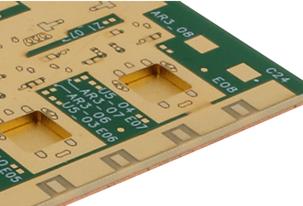
Another important aspect of heavy copper PCB manufacturing is the drilling process.
The presence of thick copper layers necessitates the use of advanced drilling techniques to create precise vias and holes. Laser drilling is often employed due to its ability to produce clean and accurate holes without damaging the surrounding material. This precision is vital for ensuring reliable electrical connections and minimizing signal loss.
Moreover, the solder mask application in heavy copper PCBs requires careful consideration.
The increased copper thickness can lead to uneven surfaces, which may affect the adhesion of the solder mask. To counter this, manufacturers often use specialized solder mask materials and application techniques to ensure a smooth and even coating. This not only enhances the board’s aesthetic appeal but also provides essential protection against environmental factors and electrical shorts.
In conclusion, the manufacturing of heavy copper PCBs involves a series of specialized techniques designed to address the unique challenges posed by increased copper thickness. From high-speed plating and differential etching to advanced drilling and solder mask application, each step is meticulously executed to ensure the production of high-quality boards capable of meeting the demanding requirements of modern electronic applications. As technology continues to advance, the importance of heavy copper PCBs is likely to grow, underscoring the need for continued innovation in their manufacturing processes.

Applications Of Heavy Copper PCBs In High-Power Electronics
Heavy copper printed circuit boards (PCBs) have emerged as a pivotal component in the realm of high-power electronics, offering a robust solution to the challenges posed by demanding electrical and thermal conditions. These PCBs are characterized by their thick copper layers, typically ranging from 3 ounces per square foot to over 20 ounces per square foot, which significantly enhance their current-carrying capacity and thermal management capabilities. As the demand for high-power electronic applications continues to grow, the role of heavy copper PCBs becomes increasingly indispensable.
One of the primary applications of heavy copper PCBs is in power distribution systems.
In these systems, the ability to handle high current loads without overheating is crucial. Heavy copper PCBs excel in this regard, as their thick copper layers allow for efficient heat dissipation and reduced thermal stress. This makes them ideal for use in power converters, inverters, and other power management devices where reliability and performance are paramount. Furthermore, the enhanced mechanical strength of heavy copper PCBs ensures durability and longevity, even under extreme operating conditions.
In addition to power distribution, heavy copper PCBs are extensively used in the automotive industry, particularly in electric vehicles (EVs) and hybrid electric vehicles (HEVs).
The transition towards electrification in the automotive sector necessitates components that can withstand high currents and temperatures. Heavy copper PCBs meet these requirements by providing a stable platform for the integration of power electronics, such as motor controllers and battery management systems. Their ability to handle high power levels without compromising on safety or efficiency makes them a preferred choice for automotive manufacturers aiming to enhance the performance and reliability of their vehicles.
Moreover, heavy copper PCBs find significant applications in renewable energy systems, including solar power and wind energy.
In these applications, the need for efficient energy conversion and management is critical. Heavy copper PCBs facilitate this by supporting high-efficiency power converters and inverters that are essential for harnessing and distributing renewable energy. Their superior thermal management capabilities ensure that these systems operate optimally, even under fluctuating environmental conditions, thereby maximizing energy output and minimizing losses.
The telecommunications industry also benefits from the use of heavy copper PCBs, particularly in the deployment of high-power radio frequency (RF) amplifiers and base stations.
As the demand for faster and more reliable communication networks increases, the need for components that can handle high power levels becomes evident. Heavy copper PCBs provide the necessary thermal and electrical performance to support these high-power applications, ensuring consistent signal quality and network reliability.
In conclusion, the applications of heavy copper PCBs in high-power electronics are vast and varied, spanning industries such as power distribution, automotive, renewable energy, and telecommunications. Their ability to handle high currents, manage heat effectively, and provide mechanical strength makes them an essential component in the design and development of high-power electronic systems. As technology continues to advance and the demand for efficient and reliable power solutions grows, the importance of heavy copper PCBs in high-power electronics is set to increase, solidifying their role as a cornerstone in modern electronic design.
Comparing Heavy Copper PCBs To Standard PCBs: Key Differences And Benefits
In the realm of printed circuit boards (PCBs), the choice of materials and design specifications can significantly impact the performance and durability of electronic devices. Among the various types of PCBs, heavy copper boards have emerged as a specialized solution for applications requiring enhanced electrical and thermal performance. To understand the advantages of heavy copper PCBs, it is essential to compare them with standard PCBs, highlighting the key differences and benefits that set them apart.
At the core of this comparison lies the thickness of the copper used in the PCB layers.
Standard PCBs typically feature copper thicknesses ranging from 1 to 3 ounces per square foot. In contrast, heavy copper PCBs utilize copper thicknesses that exceed 3 ounces per square foot, often reaching up to 20 ounces or more. This increased copper thickness is the defining characteristic of heavy copper boards and serves as the foundation for their unique properties.
One of the primary benefits of heavy copper PCBs is their ability to handle higher current loads.
The increased copper thickness allows for wider and thicker traces, which can carry more current without overheating. This capability is particularly advantageous in applications such as power distribution, automotive electronics, and industrial control systems, where high current levels are common. By accommodating greater current densities, heavy copper PCBs reduce the risk of circuit failure due to overheating, thereby enhancing the reliability and longevity of the electronic device.
In addition to improved current handling, heavy copper PCBs offer superior thermal management.
The thicker copper layers facilitate more efficient heat dissipation, which is crucial in high-power applications where excessive heat generation can compromise performance and safety. By effectively managing heat, heavy copper boards help maintain optimal operating temperatures, thus preventing thermal stress and potential damage to sensitive components. This thermal advantage is especially beneficial in environments with fluctuating temperatures or where active cooling solutions are impractical.
Moreover, heavy copper PCBs exhibit enhanced mechanical strength and durability.
The robust copper layers provide additional support to the PCB structure, making it more resistant to mechanical stresses such as bending, vibration, and thermal cycling. This increased durability is vital in applications subjected to harsh conditions, such as aerospace, military, and heavy machinery, where reliability is paramount. The ability to withstand physical and environmental challenges ensures that heavy copper PCBs maintain their integrity and functionality over extended periods.
While the benefits of heavy copper PCBs are substantial, it is important to consider the associated costs.
The manufacturing process for heavy copper boards is more complex and resource-intensive than that of standard PCBs, leading to higher production costs. However, the long-term advantages in terms of performance, reliability, and lifespan often justify the initial investment, particularly in critical applications where failure is not an option.
In conclusion, heavy copper PCBs offer distinct advantages over standard PCBs, primarily due to their increased copper thickness. The ability to handle higher current loads, superior thermal management, and enhanced mechanical strength make them an ideal choice for demanding applications. Although they come with higher production costs, the benefits they provide in terms of reliability and performance make them a worthwhile investment for industries that require robust and efficient electronic solutions. As technology continues to advance, the role of heavy copper PCBs in powering the next generation of electronic devices is likely to expand, underscoring their importance in the ever-evolving landscape of electronics.