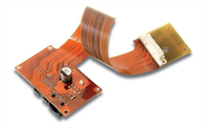
Heavy copper flex pcb
Advantages Of Heavy Copper Flex PCB In High-Current Applications
Heavy copper flex PCBs, or printed circuit boards, have emerged as a pivotal innovation in the realm of high-current applications, offering a multitude of advantages that cater to the demanding needs of modern electronic systems. As industries continue to push the boundaries of technology, the need for robust and efficient power distribution solutions becomes increasingly critical. Heavy copper flex PCBs, characterized by their thick copper layers, provide a compelling solution to these challenges, ensuring reliability and performance in high-current environments.
One of the primary advantages of heavy copper flex PCBs is their ability to handle significantly higher current loads compared to standard PCBs.
The increased copper thickness allows for greater current-carrying capacity, which is essential in applications where high power is a prerequisite. This capability not only enhances the performance of the electronic device but also ensures its longevity by reducing the risk of overheating and potential failure. Consequently, industries such as automotive, aerospace, and industrial equipment, where high-current applications are prevalent, benefit immensely from the integration of heavy copper flex PCBs.
Moreover, the flexibility of these PCBs offers an additional layer of advantage.
Unlike rigid PCBs, heavy copper flex PCBs can be bent and shaped to fit into compact and irregular spaces, making them ideal for applications where space constraints are a concern. This flexibility does not compromise their structural integrity, as the robust design ensures that the PCB can withstand mechanical stress and vibrations. As a result, they are particularly useful in environments where movement and dynamic conditions are present, such as in automotive and aerospace applications.
In addition to their mechanical benefits, heavy copper flex PCBs also contribute to improved thermal management.
The thick copper layers facilitate efficient heat dissipation, which is crucial in high-current applications where excessive heat generation can be a significant issue. By effectively managing heat, these PCBs help maintain optimal operating temperatures, thereby enhancing the overall efficiency and reliability of the electronic system. This thermal advantage is particularly beneficial in applications that require continuous operation under high power loads, as it minimizes the risk of thermal-related failures.
Furthermore, the use of heavy copper flex PCBs can lead to cost savings in the long run.
Although the initial manufacturing costs may be higher due to the increased material usage and complexity, the durability and reliability of these PCBs reduce the need for frequent replacements and repairs. This longevity translates into lower maintenance costs and less downtime, which is a critical consideration for industries where operational efficiency is paramount.
In conclusion, heavy copper flex PCBs offer a range of advantages that make them an indispensable component in high-current applications. Their ability to handle high current loads, coupled with their flexibility, thermal management capabilities, and cost-effectiveness, positions them as a superior choice for industries seeking reliable and efficient power distribution solutions. As technology continues to evolve, the demand for such advanced PCB solutions is likely to grow, further cementing the role of heavy copper flex PCBs in the future of electronic design and manufacturing.
Design Considerations For Heavy Copper Flex PCB
When designing heavy copper flex PCBs, several critical considerations must be taken into account to ensure optimal performance and reliability. Heavy copper flex PCBs, characterized by their thick copper layers, are increasingly used in applications requiring high current carrying capacity and enhanced thermal management. As such, understanding the unique design requirements of these PCBs is essential for engineers and designers.
To begin with, the choice of materials plays a pivotal role in the design of heavy copper flex PCBs.
The substrate material must be flexible enough to accommodate the bending and flexing inherent in these applications, yet robust enough to support the weight and thickness of the heavy copper layers. Polyimide is a common choice due to its excellent thermal stability and flexibility. However, the selection of adhesive materials is equally important, as they must withstand the thermal and mechanical stresses without delaminating.
Transitioning to the electrical considerations, the thickness of the copper layers is a defining characteristic of heavy copper flex PCBs.
These layers, often exceeding 3 ounces per square foot, allow for higher current carrying capacity and improved heat dissipation. However, this increased thickness necessitates careful attention to trace width and spacing to prevent issues such as overheating and short circuits. Designers must calculate the appropriate trace dimensions based on the expected current load and thermal conditions, ensuring that the PCB can handle the electrical demands without compromising performance.
Moreover, thermal management is a critical aspect of heavy copper flex PCB design.
The thick copper layers, while beneficial for heat dissipation, can also lead to uneven thermal distribution if not properly managed. To address this, designers often incorporate thermal vias and heat sinks to facilitate efficient heat transfer away from critical components. Additionally, the layout of the PCB should be optimized to minimize thermal hotspots, which can degrade performance and reduce the lifespan of the board.
Mechanical considerations are also paramount in the design of heavy copper flex PCBs.
The inherent flexibility of these boards allows them to be used in dynamic applications where movement and bending are frequent. However, the added weight of the heavy copper can introduce mechanical stress, particularly at bend points. To mitigate this, designers must carefully plan the bend radius and ensure that the copper traces are oriented in a manner that minimizes stress concentration. Furthermore, reinforcement materials may be employed in areas subject to repeated flexing to enhance durability.
In addition to these technical considerations, manufacturability is a crucial factor in the design process.
The production of heavy copper flex PCBs requires specialized techniques and equipment, as the thick copper layers can pose challenges during etching and lamination. Designers must work closely with manufacturers to ensure that the design is feasible and that any potential issues are addressed early in the development process. This collaboration can help prevent costly redesigns and ensure that the final product meets the desired specifications.
In conclusion, the design of heavy copper flex PCBs involves a complex interplay of material selection, electrical and thermal management, mechanical considerations, and manufacturability. By carefully addressing each of these aspects, designers can create PCBs that not only meet the demanding requirements of high-current applications but also offer reliability and longevity. As technology continues to advance, the importance of these design considerations will only grow, underscoring the need for expertise and precision in the development of heavy copper flex PCBs.
Manufacturing Challenges Of Heavy Copper Flex PCB
The manufacturing of heavy copper flex PCBs presents a unique set of challenges that require specialized techniques and a deep understanding of materials and processes. As the demand for more robust and reliable electronic devices increases, the need for heavy copper flex PCBs has grown, particularly in industries such as automotive, aerospace, and industrial equipment. These PCBs are characterized by their ability to handle higher current loads and provide enhanced thermal management, making them indispensable in high-performance applications. However, the path to producing these advanced circuit boards is fraught with complexities.
One of the primary challenges in manufacturing heavy copper flex PCBs is the handling of thicker copper layers.
Standard PCBs typically use copper layers ranging from 1 to 3 ounces per square foot, but heavy copper PCBs can have layers exceeding 4 ounces. This increase in copper thickness necessitates adjustments in the etching process. Traditional etching techniques may not suffice, as they can lead to uneven edges and undercuts, compromising the integrity of the circuit. Therefore, manufacturers must employ advanced etching methods, such as differential etching, to ensure precision and maintain the desired circuit patterns.
Moreover, the increased copper thickness impacts the lamination process.
The lamination of heavy copper flex PCBs requires careful control of temperature and pressure to prevent defects such as delamination or warping. The presence of thick copper layers can lead to uneven heat distribution during lamination, which can cause the dielectric materials to expand or contract unevenly. To mitigate these issues, manufacturers often use specialized materials and adhesives that can withstand the thermal stresses associated with heavy copper layers.
In addition to these technical challenges, the mechanical properties of heavy copper flex PCBs pose another set of difficulties.
Flex PCBs are designed to bend and flex without breaking, but the addition of heavy copper can reduce their flexibility. This necessitates a delicate balance between maintaining the mechanical flexibility of the board and ensuring its electrical performance. Manufacturers must carefully design the layout and choose appropriate materials to achieve this balance, often resorting to simulations and modeling to predict the behavior of the PCB under various conditions.
Furthermore, the soldering process for heavy copper flex PCBs requires particular attention.
The increased thermal mass of the thick copper layers can lead to difficulties in achieving proper solder joints. The high thermal conductivity of copper can cause rapid heat dissipation, making it challenging to maintain the necessary temperatures for soldering. To address this, manufacturers may need to adjust their soldering techniques, such as using higher temperature profiles or employing selective soldering methods to ensure reliable connections.
Finally, quality control and testing of heavy copper flex PCBs are critical to ensure their performance and reliability.
The complexity of these boards necessitates rigorous testing procedures, including thermal cycling, mechanical stress testing, and electrical performance evaluations. These tests help identify potential weaknesses and ensure that the PCBs can withstand the demanding conditions of their intended applications.
In conclusion, the manufacturing of heavy copper flex PCBs involves a series of intricate challenges that require specialized knowledge and techniques. From handling thicker copper layers to ensuring mechanical flexibility and reliable soldering, each step in the process demands careful consideration and precision. As technology continues to advance, the ability to overcome these challenges will be crucial in meeting the growing demand for high-performance electronic devices.
Innovations In Heavy Copper Flex PCB Technology
Heavy copper flex PCBs, or printed circuit boards, represent a significant advancement in the realm of electronic design and manufacturing. These innovative components are characterized by their ability to handle higher currents and dissipate heat more effectively than traditional PCBs, making them indispensable in applications that demand robust performance and reliability. As technology continues to evolve, the innovations in heavy copper flex PCB technology are paving the way for more efficient and durable electronic devices.
One of the primary innovations in heavy copper flex PCB technology is the enhancement of current-carrying capacity.
Traditional PCBs often struggle with high current loads, leading to potential overheating and failure. However, heavy copper flex PCBs are designed with thicker copper layers, which allow them to conduct higher currents without compromising the integrity of the board. This capability is particularly beneficial in industries such as automotive, aerospace, and industrial equipment, where electronic components are subjected to extreme conditions and must perform reliably over extended periods.
In addition to improved current handling, heavy copper flex PCBs offer superior thermal management.
The thicker copper layers not only facilitate better heat dissipation but also enhance the overall thermal conductivity of the board. This is crucial in applications where heat generation is a concern, such as power electronics and LED lighting systems. By effectively managing heat, these PCBs help prevent thermal-related failures and extend the lifespan of electronic devices.
Moreover, the flexibility of these PCBs adds another layer of innovation.
Unlike rigid PCBs, heavy copper flex PCBs can be bent and shaped to fit into compact and irregular spaces. This flexibility is particularly advantageous in modern electronic devices, which are becoming increasingly compact and complex. The ability to conform to various shapes without losing functionality allows designers to create more intricate and space-efficient designs, ultimately leading to more versatile and adaptable electronic products.
Another noteworthy advancement in heavy copper flex PCB technology is the improvement in manufacturing techniques.
Recent developments have led to more precise and efficient fabrication processes, enabling the production of PCBs with even thicker copper layers and more complex designs. These advancements not only enhance the performance of the PCBs but also reduce production costs and time, making them more accessible to a wider range of industries.
Furthermore, the integration of advanced materials and technologies has contributed to the evolution of heavy copper flex PCBs.
For instance, the use of high-performance substrates and advanced adhesive systems has improved the mechanical strength and reliability of these boards. Additionally, the incorporation of cutting-edge technologies such as laser drilling and precision etching has allowed for the creation of more intricate and high-density circuit patterns, further expanding the potential applications of heavy copper flex PCBs.
In conclusion, the innovations in heavy copper flex PCB technology are driving significant advancements in the electronics industry. By enhancing current-carrying capacity, improving thermal management, and offering greater design flexibility, these PCBs are meeting the demands of modern electronic applications. As manufacturing techniques continue to evolve and new materials are introduced, the potential for heavy copper flex PCBs will only grow, opening up new possibilities for electronic design and functionality. This ongoing evolution underscores the importance of continued research and development in this field, as it holds the promise of even more groundbreaking innovations in the future.