Heavy copper pcb 4layer
Advantages Of Using Heavy Copper In 4-Layer PCBs
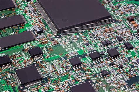
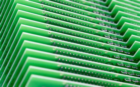
Heavy copper PCBs, particularly those with a 4-layer configuration, have become increasingly popular in various industries due to their numerous advantages. These printed circuit boards are characterized by their thick copper layers, which typically range from 3 ounces per square foot to over 20 ounces per square foot. The use of heavy copper in 4-layer PCBs offers several benefits that enhance the performance, reliability, and durability of electronic devices.
One of the primary advantages of using heavy copper in 4-layer PCBs is the improved thermal management they provide.
In electronic devices, heat dissipation is a critical factor that can significantly impact performance and longevity. Heavy copper layers facilitate efficient heat distribution across the board, reducing hotspots and preventing thermal overload.
This capability is particularly beneficial in high-power applications where excessive heat generation is a concern. By effectively managing heat, heavy copper PCBs help maintain optimal operating temperatures, thereby enhancing the overall reliability of the device.
In addition to superior thermal management, heavy copper 4-layer PCBs offer enhanced current-carrying capacity.
The increased thickness of the copper layers allows these PCBs to handle higher currents without the risk of overheating or failure. This feature is especially advantageous in applications that require high power levels, such as power supplies, automotive electronics, and industrial control systems. The ability to carry higher currents ensures that the electronic components function efficiently and safely, even under demanding conditions.
Moreover, heavy copper PCBs exhibit excellent mechanical strength and durability.
The robust construction of these boards makes them resistant to mechanical stresses, such as bending and vibration, which are common in many industrial and automotive environments. This durability translates to a longer lifespan for the electronic devices, reducing the need for frequent repairs or replacements. Consequently, the use of heavy copper in 4-layer PCBs can lead to significant cost savings over time, as the need for maintenance and downtime is minimized.
Another notable advantage of heavy copper 4-layer PCBs is their ability to support complex circuit designs.
The additional layers provide more space for routing intricate circuits, allowing for greater design flexibility. This capability is crucial in modern electronic devices, which often require compact and sophisticated circuitry to accommodate advanced functionalities. The use of heavy copper also enables the integration of multiple functions on a single board, streamlining the design process and reducing the overall size of the device.
Furthermore, heavy copper PCBs contribute to improved reliability and performance in harsh environments.
Their robust construction and enhanced thermal and electrical properties make them well-suited for applications exposed to extreme temperatures, moisture, and corrosive substances. This resilience ensures that the electronic devices continue to operate effectively, even in challenging conditions, thereby extending their operational life and maintaining consistent performance.
In conclusion, the use of heavy copper in 4-layer PCBs offers a multitude of advantages that make them an attractive choice for various high-performance applications. From superior thermal management and increased current-carrying capacity to enhanced mechanical strength and design flexibility, these PCBs provide significant benefits that enhance the reliability and efficiency of electronic devices. As technology continues to advance, the demand for heavy copper PCBs is likely to grow, driven by the need for durable and high-performing solutions in increasingly complex electronic systems.
Design Considerations For 4-Layer Heavy Copper PCBs
When designing 4-layer heavy copper printed circuit boards (PCBs), several critical considerations must be taken into account to ensure optimal performance and reliability. Heavy copper PCBs, characterized by their thick copper layers, are increasingly utilized in applications requiring high current carrying capacity and enhanced thermal management. As such, understanding the unique design requirements of these PCBs is essential for engineers and designers.
To begin with, the choice of materials plays a pivotal role in the design of 4-layer heavy copper PCBs.
The substrate material must be capable of withstanding the high temperatures associated with heavy copper applications. FR-4, a common substrate material, is often used; however, for more demanding applications, materials with higher thermal conductivity may be necessary. The selection of the appropriate substrate ensures that the PCB can handle the thermal and mechanical stresses it will encounter during operation.
Transitioning to the layout design, it is crucial to consider the distribution of copper across the layers.
In a 4-layer configuration, the inner layers are typically used for power and ground planes, while the outer layers are reserved for signal routing. The thickness of the copper layers, which can range from 3 oz/ft² to 20 oz/ft² or more, must be carefully chosen based on the current requirements and thermal performance needed. Thicker copper layers provide lower resistance paths for current flow, reducing power loss and improving efficiency.
Moreover, thermal management is a significant concern in heavy copper PCB design.
The increased copper thickness enhances the board’s ability to dissipate heat, but additional measures may still be necessary. Incorporating thermal vias, heat sinks, and thermal pads can further improve heat dissipation. These features help to prevent hotspots and ensure that the PCB operates within safe temperature limits, thereby extending its lifespan and reliability.
Another important consideration is the mechanical strength of the PCB.
The added weight of heavy copper layers can impose additional stress on the board, particularly during handling and assembly. To mitigate this, designers must ensure that the board’s mechanical structure is robust enough to support the increased weight. This may involve reinforcing the board with additional support structures or selecting a thicker substrate material.
Furthermore, the manufacturing process for heavy copper PCBs requires specialized techniques.
The etching process, for instance, must be carefully controlled to achieve precise copper patterns without over-etching. This is particularly important for maintaining the integrity of fine features and ensuring that the board meets its electrical specifications. Additionally, the plating process must be optimized to ensure uniform copper thickness across the board.
In conclusion, designing 4-layer heavy copper PCBs involves a comprehensive understanding of material selection, thermal management, mechanical strength, and manufacturing processes. By carefully considering these factors, designers can create PCBs that meet the demanding requirements of high-power applications. As technology continues to advance, the role of heavy copper PCBs in providing reliable and efficient solutions will undoubtedly grow, making it imperative for designers to stay informed about the latest developments and best practices in this field.
Applications Of Heavy Copper 4-Layer PCBs In Power Electronics
Heavy copper 4-layer printed circuit boards (PCBs) have become increasingly significant in the realm of power electronics, offering a robust solution for applications that demand high current carrying capacity and enhanced thermal management. These PCBs are characterized by their thick copper layers, typically ranging from 3 oz/ft² to 20 oz/ft², which provide superior electrical conductivity and mechanical strength. As power electronics continue to evolve, the demand for heavy copper PCBs has surged, driven by their ability to handle higher currents and dissipate heat more effectively than standard PCBs.
One of the primary applications of heavy copper 4-layer PCBs is in power supply systems.
These systems require efficient power distribution and reliable performance under high current loads. Heavy copper PCBs excel in this regard, as their thick copper layers allow for the distribution of large currents without the risk of overheating or failure. This makes them ideal for use in uninterruptible power supplies (UPS), power converters, and inverters, where maintaining a stable power output is crucial.
Moreover, heavy copper 4-layer PCBs are extensively used in the automotive industry, particularly in electric vehicles (EVs) and hybrid electric vehicles (HEVs).
The automotive sector demands components that can withstand harsh environmental conditions and provide consistent performance. Heavy copper PCBs meet these requirements by offering enhanced thermal management, which is essential for the efficient operation of power modules and battery management systems in EVs and HEVs. Their ability to handle high power levels ensures that these vehicles can operate safely and efficiently, even under demanding conditions.
In addition to automotive applications, heavy copper 4-layer PCBs are also prevalent in renewable energy systems, such as solar power and wind energy installations.
These systems require components that can manage high power outputs and endure fluctuating environmental conditions. Heavy copper PCBs are well-suited for these applications due to their durability and ability to conduct high currents with minimal energy loss. In solar inverters, for instance, they facilitate the conversion of direct current (DC) to alternating current (AC) with high efficiency, thereby maximizing the energy yield from solar panels.
Furthermore, heavy copper 4-layer PCBs find applications in industrial equipment, where they are used in motor drives, power distribution units, and high-power rectifiers.
The industrial sector often involves equipment that operates under high power loads and requires reliable performance over extended periods. Heavy copper PCBs provide the necessary robustness and thermal management capabilities to ensure that these systems function optimally, reducing the risk of downtime and maintenance costs.
In conclusion, the applications of heavy copper 4-layer PCBs in power electronics are diverse and critical to the advancement of various industries. Their ability to handle high currents, provide excellent thermal management, and offer mechanical strength makes them indispensable in power supply systems, automotive applications, renewable energy installations, and industrial equipment. As technology continues to advance, the role of heavy copper PCBs in power electronics is expected to grow, driven by the increasing demand for efficient, reliable, and high-performance electronic components.
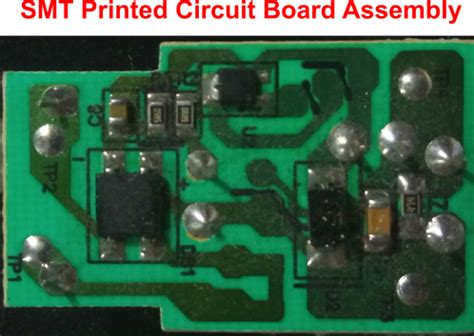
Manufacturing Challenges And Solutions For Heavy Copper 4-Layer PCBs
The manufacturing of heavy copper 4-layer printed circuit boards (PCBs) presents a unique set of challenges that require specialized solutions to ensure optimal performance and reliability. As electronic devices become more complex and power-intensive, the demand for PCBs capable of handling higher current loads and dissipating heat efficiently has increased. Heavy copper PCBs, characterized by copper thicknesses greater than 3 ounces per square foot, are particularly suited for these applications. However, their production involves several intricate processes that must be carefully managed to overcome inherent difficulties.
One of the primary challenges in manufacturing heavy copper 4-layer PCBs is the etching process.
Standard etching techniques, which work well for thinner copper layers, are often inadequate for heavy copper due to the increased material thickness. The etching process must be precisely controlled to ensure that the desired circuit patterns are accurately formed without over-etching, which can lead to defects such as undercuts or uneven edges. To address this, manufacturers often employ advanced etching solutions and techniques, such as differential etching, which allows for more precise control over the removal of copper material.
In addition to etching, the lamination process poses another significant challenge.
The increased copper thickness can lead to difficulties in achieving proper adhesion between layers, which is crucial for the structural integrity and electrical performance of the PCB. To mitigate this issue, manufacturers may use high-pressure lamination techniques and specialized bonding materials that enhance adhesion. Furthermore, careful attention must be paid to the thermal management during lamination, as the thicker copper layers can lead to uneven heat distribution, potentially causing warping or delamination.
Drilling is another critical step in the production of heavy copper 4-layer PCBs that requires specialized attention.
The increased copper thickness can cause excessive wear on drilling tools, leading to higher tool costs and potential delays in production. To address this, manufacturers often utilize advanced drilling equipment with enhanced durability and precision. Additionally, optimizing drilling parameters, such as speed and feed rate, can help minimize tool wear and improve hole quality.
Moreover, the plating process for heavy copper PCBs is more complex than for standard PCBs.
The thicker copper layers require more substantial plating to ensure adequate coverage and connectivity between layers. This necessitates the use of specialized plating baths and techniques to achieve uniform deposition without introducing defects such as voids or uneven thickness. Manufacturers may also employ pulse plating techniques, which allow for better control over the deposition process and result in more consistent layer thickness.
Despite these challenges, the demand for heavy copper 4-layer PCBs continues to grow, driven by their ability to handle high power loads and provide superior thermal management.
To meet this demand, manufacturers are continually innovating and refining their processes. By investing in advanced equipment and developing new techniques, they can overcome the inherent difficulties associated with heavy copper PCB production. As a result, they are able to deliver high-quality products that meet the stringent requirements of modern electronic applications.
In conclusion, while the manufacturing of heavy copper 4-layer PCBs presents several challenges, these can be effectively addressed through the use of advanced techniques and equipment. By understanding and overcoming these challenges, manufacturers can produce reliable and efficient PCBs that meet the needs of today’s power-intensive electronic devices.


