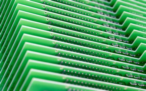
Heavy copper pcb factories
Advantages Of Heavy Copper PCBs In Industrial Applications
Heavy copper PCBs, characterized by their thick copper layers, have become increasingly significant in industrial applications due to their unique advantages. These printed circuit boards are distinguished by copper weights exceeding three ounces per square foot, which is considerably thicker than the copper layers found in standard PCBs. This increased thickness imparts several benefits that are particularly valuable in demanding industrial environments.
One of the primary advantages of heavy copper PCBs is their enhanced current-carrying capacity.
In industrial applications, where high power levels are often required, the ability to handle substantial current loads without overheating is crucial. The thick copper layers in these PCBs allow for efficient heat dissipation, reducing the risk of thermal damage and ensuring reliable performance even under high-stress conditions. This capability is particularly beneficial in power electronics, where maintaining optimal thermal management is essential for the longevity and efficiency of the components.
Moreover, heavy copper PCBs offer superior mechanical strength, which is a critical factor in industrial settings.
The robust construction of these boards makes them resistant to mechanical stresses such as vibrations and shocks, which are common in industrial environments. This durability ensures that the PCBs can withstand harsh conditions without compromising their functionality, thereby reducing the likelihood of failures and the associated downtime. Consequently, industries that rely on heavy machinery and equipment can benefit significantly from the reliability and longevity provided by heavy copper PCBs.
In addition to their mechanical and thermal advantages, heavy copper PCBs also facilitate complex circuit designs.
The increased copper thickness allows for the integration of multiple layers and intricate circuit patterns, enabling the design of compact and efficient systems. This capability is particularly advantageous in applications where space is limited, yet high performance is required. By accommodating complex circuitry within a smaller footprint, heavy copper PCBs contribute to the development of advanced industrial systems that are both powerful and efficient.
Furthermore, the use of heavy copper PCBs can lead to cost savings in the long run.
Although the initial manufacturing costs may be higher compared to standard PCBs, the durability and reliability of heavy copper boards often result in lower maintenance and replacement costs. Industries can benefit from reduced operational disruptions and extended equipment lifespans, ultimately leading to improved cost-effectiveness over time. This economic advantage is a compelling reason for industries to consider heavy copper PCBs for their critical applications.
In conclusion, the advantages of heavy copper PCBs in industrial applications are manifold.
Their ability to handle high current loads, coupled with superior thermal and mechanical properties, makes them an ideal choice for demanding environments. The capacity to support complex circuit designs further enhances their appeal, allowing for the development of sophisticated and efficient systems. While the initial investment may be higher, the long-term benefits in terms of reliability, durability, and cost savings make heavy copper PCBs a valuable asset in industrial applications. As industries continue to evolve and demand more robust and efficient solutions, the role of heavy copper PCBs is likely to become even more prominent, underscoring their importance in the advancement of industrial technology.

Innovations In Heavy Copper PCB Manufacturing Techniques
In recent years, the demand for heavy copper printed circuit boards (PCBs) has surged, driven by their ability to handle higher currents and provide enhanced thermal management. This demand has spurred significant innovations in manufacturing techniques, allowing factories to produce heavy copper PCBs with greater efficiency and precision. As the industry evolves, these advancements are reshaping the landscape of PCB manufacturing, offering new possibilities for applications in various sectors, including automotive, aerospace, and industrial electronics.
One of the most notable innovations in heavy copper PCB manufacturing is the development of advanced etching techniques.
Traditional etching methods often struggle with the increased thickness of heavy copper layers, leading to issues such as uneven etching and reduced precision. However, recent advancements have introduced more sophisticated etching processes that utilize chemical and mechanical methods to achieve uniformity and accuracy. These techniques not only improve the quality of the final product but also reduce material waste, making the manufacturing process more sustainable.
In addition to etching, the plating process has also seen significant improvements.
Electroplating, a critical step in PCB manufacturing, has been refined to accommodate the unique challenges posed by heavy copper layers. Innovations in electroplating chemistry and equipment have enabled manufacturers to achieve thicker and more uniform copper deposits. This advancement is crucial for ensuring the structural integrity and electrical performance of heavy copper PCBs, particularly in applications where reliability is paramount.
Moreover, the integration of automation and digital technologies has revolutionized the production of heavy copper PCBs.
Automated systems equipped with advanced sensors and machine learning algorithms are now capable of monitoring and controlling various aspects of the manufacturing process in real-time. This level of precision ensures that each PCB meets stringent quality standards while minimizing human error. Furthermore, digital twin technology allows manufacturers to simulate and optimize production processes before actual implementation, reducing downtime and enhancing overall efficiency.
Another significant innovation is the use of advanced materials in the construction of heavy copper PCBs.
The development of high-performance substrates and dielectric materials has enabled manufacturers to produce PCBs that can withstand extreme conditions, such as high temperatures and mechanical stress. These materials not only enhance the durability of the PCBs but also contribute to improved thermal management, a critical factor in high-power applications. As a result, heavy copper PCBs are now more versatile and reliable than ever before.
Furthermore, the push towards sustainability has led to the adoption of environmentally friendly practices in heavy copper PCB manufacturing.
Factories are increasingly implementing green technologies, such as water recycling systems and energy-efficient machinery, to reduce their environmental footprint. Additionally, the use of lead-free solder and other eco-friendly materials is becoming more prevalent, aligning with global efforts to promote sustainable manufacturing practices.
In conclusion, the innovations in heavy copper PCB manufacturing techniques are transforming the industry, offering enhanced performance, reliability, and sustainability. As these advancements continue to evolve, they will undoubtedly open new avenues for applications across various sectors, driving further growth and development. The integration of cutting-edge technologies and materials not only addresses the challenges associated with heavy copper PCBs but also sets the stage for future innovations, ensuring that the industry remains at the forefront of technological progress.
Environmental Impact Of Heavy Copper PCB Production
The production of heavy copper printed circuit boards (PCBs) is a critical component in the electronics industry, particularly for applications requiring high power and thermal management. However, the environmental impact of this manufacturing process is a growing concern.
Heavy copper PCBs, characterized by their thick copper layers, are essential for high-current applications, but their production involves several environmentally challenging processes. Understanding these impacts is crucial for developing more sustainable practices in the industry.
To begin with, the extraction and processing of copper, a primary material in heavy copper PCBs, have significant environmental implications.
Mining activities often lead to habitat destruction, soil erosion, and water pollution due to the release of toxic substances. Furthermore, the energy-intensive nature of copper extraction and refining contributes to greenhouse gas emissions, exacerbating climate change. As the demand for heavy copper PCBs increases, so does the pressure on natural resources, highlighting the need for more efficient and sustainable mining practices.
In addition to the raw material extraction, the manufacturing process of heavy copper PCBs itself poses environmental challenges.
The production involves several chemical processes, including etching and plating, which utilize hazardous chemicals such as sulfuric acid and hydrogen peroxide. These chemicals, if not managed properly, can lead to environmental contamination. Wastewater generated during the manufacturing process often contains heavy metals and other pollutants, which can harm aquatic ecosystems if discharged untreated. Consequently, factories must implement stringent waste management and treatment protocols to mitigate these impacts.
Moreover, the energy consumption associated with heavy copper PCB production is another significant environmental concern.
The manufacturing process requires substantial energy input, primarily from non-renewable sources, contributing to carbon emissions. As the electronics industry continues to grow, the cumulative energy demand from PCB production is expected to rise, underscoring the importance of adopting energy-efficient technologies and renewable energy sources in manufacturing facilities.
Transitioning to the end-of-life stage, heavy copper PCBs also present challenges in terms of waste management.
Electronic waste, or e-waste, is a rapidly growing waste stream, and heavy copper PCBs contribute to this issue. Improper disposal of e-waste can lead to the release of toxic substances into the environment, posing risks to human health and ecosystems. Recycling heavy copper PCBs is a complex process due to the intricate design and the presence of various materials. However, improving recycling technologies and promoting circular economy principles can help mitigate the environmental impact of e-waste.
In light of these challenges, it is imperative for heavy copper PCB factories to adopt more sustainable practices.
This includes investing in cleaner production technologies, improving resource efficiency, and enhancing waste management systems. Additionally, collaboration with stakeholders across the supply chain can drive innovation and the development of eco-friendly materials and processes. Policymakers also play a crucial role by implementing regulations and incentives that encourage sustainable practices in the industry.
In conclusion, while heavy copper PCBs are indispensable for modern electronics, their production poses significant environmental challenges. Addressing these issues requires a concerted effort from manufacturers, policymakers, and consumers alike. By prioritizing sustainability, the industry can reduce its environmental footprint and contribute to a more sustainable future.
Quality Control Measures In Heavy Copper PCB Factories
In the realm of electronics manufacturing, heavy copper printed circuit boards (PCBs) play a crucial role due to their ability to handle higher currents and provide enhanced thermal management. As the demand for these robust PCBs continues to rise, ensuring their quality becomes paramount. Heavy copper PCB factories implement a series of stringent quality control measures to maintain the integrity and performance of their products. These measures are essential not only for meeting industry standards but also for ensuring customer satisfaction and safety.
To begin with, the selection of raw materials is a critical step in the quality control process.
Factories source high-quality copper and substrate materials to ensure that the final product can withstand the demanding conditions it is designed for. The copper used must have the appropriate thickness and purity to handle the increased electrical loads. By starting with superior materials, manufacturers lay a solid foundation for producing reliable heavy copper PCBs.
Following the procurement of materials, the manufacturing process itself is subject to rigorous oversight.
Advanced machinery and technology are employed to ensure precision in the etching and layering processes. Automated systems are often used to apply copper layers uniformly, which is crucial for maintaining consistent electrical performance across the board. Moreover, these systems are regularly calibrated and maintained to prevent any deviations that could compromise the quality of the PCBs.
In addition to automated processes, human oversight remains a vital component of quality control.
Skilled technicians conduct visual inspections at various stages of production to identify any defects or irregularities. These inspections are complemented by automated optical inspection (AOI) systems, which use high-resolution cameras and sophisticated algorithms to detect even the smallest anomalies. By combining human expertise with technological advancements, factories can ensure a higher level of accuracy in defect detection.
Furthermore, electrical testing is a cornerstone of quality assurance in heavy copper PCB manufacturing.
Each board undergoes a series of tests to verify its electrical properties, such as conductivity and resistance. These tests are crucial for confirming that the PCBs can handle the specified current loads without failure. In some cases, thermal cycling tests are also conducted to assess the board’s ability to withstand temperature fluctuations, which is particularly important for applications involving high power and heat dissipation.
Another significant aspect of quality control is the adherence to industry standards and certifications.
Heavy copper PCB factories often seek certifications such as ISO 9001, which demonstrates their commitment to maintaining a high standard of quality management. Compliance with these standards ensures that the manufacturing processes are consistent, efficient, and capable of producing reliable products. Additionally, these certifications provide customers with confidence in the factory’s ability to deliver PCBs that meet their specific requirements.
Finally, continuous improvement is a hallmark of successful heavy copper PCB factories.
By analyzing data from quality control processes and customer feedback, manufacturers can identify areas for enhancement. This proactive approach allows them to refine their processes, reduce waste, and improve product quality over time. In conclusion, the quality control measures implemented in heavy copper PCB factories are comprehensive and multifaceted, encompassing everything from material selection to final testing. Through a combination of advanced technology, skilled personnel, and adherence to industry standards, these factories ensure that their products meet the highest levels of quality and reliability.


