Heavy copper pcb vacuum high voltage
Advantages Of Heavy Copper PCB In High Voltage Applications
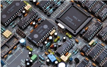
In the realm of high voltage applications, the utilization of heavy copper printed circuit boards (PCBs) has emerged as a significant advancement, offering numerous advantages that enhance performance and reliability. Heavy copper PCBs, characterized by their thicker copper layers compared to standard PCBs, are increasingly favored in industries where high voltage and high current are prevalent. This preference is driven by several key benefits that heavy copper PCBs provide, making them indispensable in demanding electrical environments.
One of the primary advantages of heavy copper PCBs in high voltage applications is their superior thermal management capabilities.
The increased copper thickness allows for better heat dissipation, which is crucial in high voltage scenarios where excessive heat generation can lead to component failure or reduced efficiency. By effectively managing heat, heavy copper PCBs help maintain optimal operating temperatures, thereby enhancing the longevity and reliability of the electronic components they support. This is particularly important in applications such as power distribution, automotive electronics, and industrial machinery, where consistent performance is critical.
Moreover, heavy copper PCBs offer enhanced mechanical strength, which is vital in high voltage applications that often involve harsh operating conditions.
The robust construction of these PCBs ensures they can withstand mechanical stresses, such as vibrations and shocks, without compromising their structural integrity. This durability is essential in environments where equipment is subject to constant movement or potential physical impact, ensuring that the electrical connections remain secure and reliable over time.
In addition to thermal and mechanical benefits, heavy copper PCBs provide improved electrical conductivity.
The thicker copper layers reduce the resistance of the electrical pathways, allowing for more efficient current flow. This is particularly advantageous in high voltage applications where minimizing energy loss is crucial for maintaining system efficiency. The reduced resistance also contributes to lower power consumption, which can lead to cost savings and increased energy efficiency in the long run.
Furthermore, heavy copper PCBs enable the design of more compact and efficient circuits.
The ability to handle higher currents and voltages without the need for additional components or larger board sizes allows engineers to create more streamlined and space-efficient designs. This is especially beneficial in applications where space is at a premium, such as in aerospace and telecommunications, where compact and lightweight solutions are highly valued.
Another notable advantage of heavy copper PCBs is their ability to support complex circuit designs.
The increased copper thickness allows for the integration of multiple layers and intricate routing patterns, facilitating the development of sophisticated electronic systems. This capability is essential in high voltage applications that require advanced functionality and precise control, such as in renewable energy systems and electric vehicles.
In conclusion, the advantages of heavy copper PCBs in high voltage applications are manifold, encompassing superior thermal management, enhanced mechanical strength, improved electrical conductivity, and the ability to support complex circuit designs. These benefits make heavy copper PCBs an ideal choice for industries that demand high performance and reliability in challenging electrical environments. As technology continues to advance, the role of heavy copper PCBs in high voltage applications is likely to expand, further solidifying their importance in the development of innovative and efficient electronic systems.
Manufacturing Techniques For Heavy Copper PCBs In Vacuum Environments
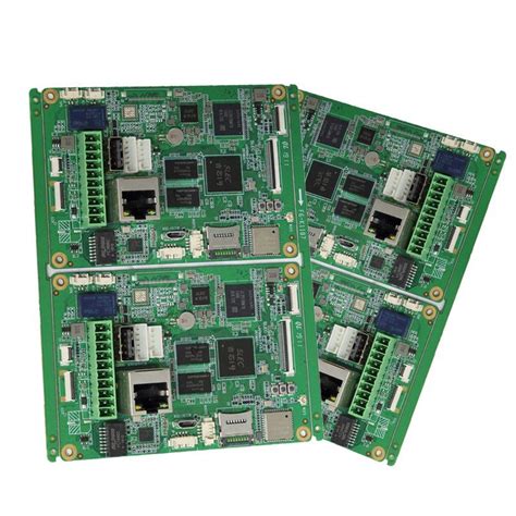
In the realm of advanced electronics, the demand for heavy copper printed circuit boards (PCBs) has surged, particularly in applications requiring high voltage and high current. These specialized PCBs are integral to industries such as power electronics, automotive, and renewable energy, where they are valued for their ability to handle substantial electrical loads while maintaining structural integrity. The manufacturing of heavy copper PCBs, especially in vacuum environments, involves a series of sophisticated techniques that ensure optimal performance and reliability.
To begin with, heavy copper PCBs are characterized by their thick copper layers, typically ranging from 3 oz/ft² to 20 oz/ft² or more.
This increased copper thickness allows for enhanced current carrying capacity and improved thermal management, which are crucial in high voltage applications. The manufacturing process of these PCBs in vacuum environments starts with the selection of appropriate base materials. High-quality substrates, such as FR-4 or polyimide, are chosen for their excellent dielectric properties and thermal stability. These materials must withstand the rigors of high voltage operations while maintaining their structural integrity.
Once the substrate is selected, the next step involves the application of copper layers.
In vacuum environments, techniques such as vacuum deposition or sputtering are employed to ensure uniform copper layer distribution. These methods offer superior adhesion and precision compared to traditional electroplating, which is critical for heavy copper applications. Vacuum deposition, in particular, allows for the controlled deposition of copper atoms onto the substrate, resulting in a dense and uniform copper layer that enhances the PCB’s electrical and thermal performance.
Following the deposition of copper layers, the etching process is employed to define the circuit patterns.
In vacuum environments, dry etching techniques, such as plasma etching, are preferred over wet chemical etching. Plasma etching offers greater precision and control, which is essential for creating intricate circuit patterns on heavy copper PCBs. This method also minimizes the risk of undercutting, a common issue in wet etching that can compromise the integrity of the circuit paths.
Subsequently, the PCBs undergo a series of lamination processes to build up the desired number of layers.
In vacuum environments, the lamination process benefits from reduced oxidation and contamination, resulting in stronger interlayer bonds. This is particularly important for heavy copper PCBs, as the increased copper thickness can pose challenges in achieving reliable layer adhesion. Vacuum lamination ensures that the layers are bonded with minimal voids, enhancing the mechanical strength and electrical performance of the final product.
Finally, the heavy copper PCBs are subjected to rigorous testing to ensure they meet the stringent requirements of high voltage applications.
Electrical testing, thermal cycling, and mechanical stress tests are conducted to verify the PCBs’ performance under extreme conditions. The vacuum environment during manufacturing plays a crucial role in enhancing the reliability of these tests, as it reduces the presence of contaminants that could affect the results.
In conclusion, the manufacturing of heavy copper PCBs in vacuum environments involves a series of advanced techniques that ensure the production of high-performance, reliable circuit boards. From the selection of base materials to the application of copper layers and the precision etching of circuit patterns, each step is meticulously controlled to meet the demands of high voltage applications. As industries continue to push the boundaries of electronic performance, the role of heavy copper PCBs manufactured in vacuum environments will undoubtedly become increasingly significant.
Design Considerations For High Voltage Heavy Copper PCBs
When designing high voltage heavy copper printed circuit boards (PCBs), several critical considerations must be taken into account to ensure optimal performance and reliability. Heavy copper PCBs, characterized by their thick copper layers, are particularly suited for high voltage applications due to their enhanced current carrying capacity and superior thermal management. As such, understanding the unique design requirements for these PCBs is essential for engineers and designers working in fields such as power electronics, automotive, and industrial applications.
To begin with, the choice of materials plays a pivotal role in the design of high voltage heavy copper PCBs.
The substrate material must possess excellent dielectric properties to withstand high voltage levels without breakdown. FR-4, a commonly used substrate, may not always be suitable for very high voltage applications, necessitating the use of alternative materials such as polyimide or ceramic-based substrates. These materials offer better thermal stability and dielectric strength, which are crucial for maintaining the integrity of the PCB under high voltage conditions.
Moreover, the thickness of the copper layers is a fundamental aspect of heavy copper PCB design.
Typically, copper thicknesses range from 3 oz/ft² to 20 oz/ft² or more, depending on the specific application requirements. Thicker copper layers allow for higher current carrying capacity and improved heat dissipation, which are essential for preventing overheating and ensuring the longevity of the PCB. However, it is important to balance the copper thickness with the overall design to avoid excessive weight and cost.
In addition to material selection and copper thickness, the layout of the PCB is another critical consideration.
Proper spacing between conductive traces is essential to prevent arcing and ensure electrical isolation. The spacing must be carefully calculated based on the operating voltage and environmental conditions, such as humidity and temperature. Furthermore, the use of wider traces and larger pads can help distribute current more evenly, reducing the risk of localized heating and potential failure points.
Thermal management is another key factor in the design of high voltage heavy copper PCBs.
Efficient heat dissipation is vital to prevent thermal stress and maintain the performance of the board. Techniques such as the use of thermal vias, heat sinks, and thermal pads can be employed to enhance heat transfer away from critical components. Additionally, the integration of thermal simulation tools during the design phase can provide valuable insights into potential thermal issues and allow for proactive design adjustments.
Furthermore, the mechanical design of the PCB must also be considered.
Heavy copper PCBs are inherently more robust than their standard counterparts, but they still require careful mechanical design to withstand the stresses of high voltage applications. This includes ensuring adequate support for heavy components and considering the effects of vibration and mechanical shock.
Finally, testing and validation are crucial steps in the design process of high voltage heavy copper PCBs.
Rigorous testing under simulated operating conditions can help identify potential weaknesses and ensure that the PCB meets all necessary safety and performance standards. This includes high voltage testing, thermal cycling, and mechanical stress testing.
In conclusion, the design of high voltage heavy copper PCBs involves a comprehensive approach that considers material selection, copper thickness, layout, thermal management, mechanical design, and thorough testing. By addressing these considerations, designers can create PCBs that not only meet the demanding requirements of high voltage applications but also deliver reliable and efficient performance over their operational lifespan.
Thermal Management Solutions For Heavy Copper PCBs In High Voltage Systems
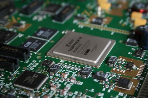
In the realm of high voltage systems, the demand for efficient thermal management solutions has become increasingly critical. Heavy copper printed circuit boards (PCBs) have emerged as a pivotal component in addressing these thermal challenges. These PCBs, characterized by their thick copper layers, are specifically designed to handle high current loads and dissipate heat effectively. As high voltage systems continue to evolve, the integration of heavy copper PCBs offers a promising avenue for enhancing performance and reliability.
To understand the significance of heavy copper PCBs in high voltage applications, it is essential to consider their unique properties.
The increased copper thickness, often ranging from 105 to 400 micrometers or more, allows these PCBs to conduct higher currents without overheating. This capability is particularly advantageous in high voltage systems where excessive heat generation can lead to component failure or reduced efficiency. By efficiently distributing heat across the board, heavy copper PCBs mitigate the risk of hotspots, thereby extending the lifespan of the system.
Moreover, the robust construction of heavy copper PCBs contributes to their ability to withstand thermal cycling and mechanical stress.
This durability is crucial in high voltage environments where fluctuations in temperature and electrical load are common. The enhanced mechanical strength of these PCBs ensures that they maintain structural integrity even under demanding conditions, reducing the likelihood of circuit failure. Consequently, heavy copper PCBs are increasingly being adopted in industries such as power electronics, automotive, and renewable energy, where reliability and performance are paramount.
In addition to their thermal management capabilities, heavy copper PCBs offer improved electrical performance.
The thick copper layers reduce the resistance of the circuit, allowing for more efficient power transmission. This reduction in resistance not only enhances the overall efficiency of the system but also minimizes energy losses, which is a critical consideration in high voltage applications. Furthermore, the ability to design complex multilayer circuits with heavy copper PCBs enables engineers to optimize the layout for better signal integrity and reduced electromagnetic interference.
Transitioning to the manufacturing aspect, the production of heavy copper PCBs involves specialized techniques to ensure precision and quality.
The process typically includes advanced etching and plating methods to achieve the desired copper thickness and pattern accuracy. Manufacturers must also employ stringent quality control measures to detect any defects that could compromise the performance of the PCB. As technology advances, innovations in manufacturing processes continue to enhance the capabilities of heavy copper PCBs, making them more accessible and cost-effective for a wider range of applications.
Looking ahead, the role of heavy copper PCBs in high voltage systems is poised to expand further.
As industries strive for greater energy efficiency and sustainability, the demand for reliable thermal management solutions will only intensify. Heavy copper PCBs, with their ability to handle high currents and dissipate heat effectively, are well-positioned to meet these evolving needs. By providing a robust platform for high voltage applications, these PCBs not only enhance system performance but also contribute to the advancement of technologies that rely on efficient power management.
In conclusion, heavy copper PCBs represent a vital component in the quest for effective thermal management solutions in high voltage systems. Their unique properties, including superior heat dissipation, mechanical strength, and electrical performance, make them indispensable in a variety of industries. As technology continues to advance, the integration of heavy copper PCBs will undoubtedly play a crucial role in shaping the future of high voltage applications, driving innovation and ensuring the reliability of critical systems.