High-Density PCB: Design, Manufacturing, and Applications
Introduction
Printed Circuit Boards (PCBs) are the backbone of modern electronics, providing the necessary platform for interconnecting electronic components. As technology advances, the demand for smaller, faster, and more efficient electronic devices has led to the development of High-Density Interconnect (HDI) PCBs. High-Density PCBs are characterized by their ability to accommodate a large number of components and interconnections in a compact space, making them ideal for applications where space and performance are critical. This article explores the design, manufacturing, and applications of High-Density PCBs, highlighting their importance in the electronics industry.
1. What is a High-Density PCB?
High-Density PCBs, also known as HDI PCBs, are a type of printed circuit board that features a higher wiring density per unit area compared to traditional PCBs. This is achieved through the use of advanced manufacturing techniques, such as microvias, fine-line tracing, and sequential lamination. The result is a PCB that can support more components and connections in a smaller footprint, enabling the development of compact and high-performance electronic devices.
2. Key Features of High-Density PCBs
2.1 Microvias
Microvias are small holes drilled into the PCB that allow for the interconnection of different layers. These vias are typically less than 150 microns in diameter and are used to create high-density interconnections between layers. Microvias can be blind (connecting an outer layer to an inner layer) or buried (connecting two inner layers), and they play a crucial role in reducing the overall size of the PCB.
2.2 Fine-Line Tracing
Fine-line tracing refers to the use of narrow traces to connect components on the PCB. High-Density PCBs often feature trace widths and spacings that are significantly smaller than those found in traditional PCBs. This allows for more traces to be routed in a given area, increasing the overall density of the board.
2.3 Sequential Lamination
Sequential lamination is a manufacturing process that involves building up the PCB layer by layer. This technique allows for the creation of complex multilayer structures with high-density interconnections. Each layer is laminated separately, and microvias are used to connect the layers, resulting in a compact and highly integrated PCB.
2.4 High Layer Count
High-Density PCBs often have a higher number of layers compared to traditional PCBs. This increased layer count allows for more complex routing and the accommodation of a greater number of components. The use of high layer counts is particularly important in applications where space is limited, such as in mobile devices and wearable technology.
3. Design Considerations for High-Density PCBs
Designing a High-Density PCB requires careful consideration of several factors to ensure optimal performance and manufacturability. Some of the key design considerations include:
3.1 Component Placement
Proper component placement is critical in High-Density PCB design. Components should be placed in a way that minimizes the length of interconnections and reduces signal interference. This often involves placing high-speed components closer to each other and ensuring that sensitive components are shielded from noise sources.
3.2 Signal Integrity
Signal integrity is a major concern in High-Density PCBs, especially in high-speed applications. Designers must consider factors such as impedance matching, crosstalk, and signal reflection to ensure that signals are transmitted accurately and without distortion. The use of controlled impedance traces and proper grounding techniques can help mitigate signal integrity issues.
3.3 Thermal Management
High-Density PCBs often generate more heat due to the increased number of components and interconnections. Effective thermal management is essential to prevent overheating and ensure the reliability of the PCB. This can be achieved through the use of thermal vias, heat sinks, and proper component spacing to allow for adequate airflow.
3.4 Manufacturability
Designing a High-Density PCB that is manufacturable requires close collaboration between the design and manufacturing teams. Designers must consider the capabilities and limitations of the manufacturing process, such as the minimum trace width, via size, and layer count. Design for Manufacturability (DFM) guidelines should be followed to ensure that the PCB can be produced reliably and cost-effectively.
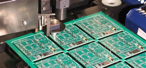
4. Manufacturing Process for High-Density PCBs
The manufacturing process for High-Density PCBs is more complex and involves several advanced techniques compared to traditional PCBs. The key steps in the manufacturing process include:
4.1 Material Selection
The choice of materials is critical in High-Density PCB manufacturing. High-performance materials with low dielectric constants and low loss tangents are often used to ensure signal integrity and reduce signal loss. Common materials include FR-4, polyimide, and Rogers materials, depending on the specific requirements of the application.
4.2 Lamination
The lamination process involves bonding multiple layers of the PCB together under heat and pressure. In High-Density PCBs, sequential lamination is often used to build up the board layer by layer. This allows for the creation of complex multilayer structures with high-density interconnections.
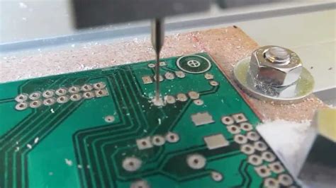
4.3 Drilling and Microvia Formation
Drilling is used to create vias that connect different layers of the PCB. In High-Density PCBs, laser drilling is often used to create microvias with diameters as small as 50 microns. Laser drilling offers greater precision and allows for the creation of blind and buried vias, which are essential for high-density interconnections.
4.4 Plating and Etching
After drilling, the vias are plated with copper to create electrical connections between layers. The PCB is then etched to remove excess copper and define the traces and pads. Advanced etching techniques, such as photolithography, are used to achieve fine-line tracing and high-density interconnections.
4.5 Surface Finish
The surface finish is applied to protect the copper traces and pads from oxidation and to ensure good solderability. Common surface finishes for High-Density PCBs include Electroless Nickel Immersion Gold (ENIG), Immersion Silver, and Organic Solderability Preservative (OSP).
4.6 Testing and Inspection
High-Density PCBs undergo rigorous testing and inspection to ensure that they meet the required specifications. Automated Optical Inspection (AOI) and X-ray inspection are commonly used to detect defects such as shorts, opens, and misaligned vias. Electrical testing is also performed to verify the functionality of the PCB.
5. Applications of High-Density PCBs
High-Density PCBs are used in a wide range of applications where space and performance are critical. Some of the key applications include:
5.1 Consumer Electronics
High-Density PCBs are widely used in consumer electronics, such as smartphones, tablets, and laptops. These devices require compact and high-performance PCBs to accommodate the increasing number of features and functionalities. High-Density PCBs enable the development of thinner and lighter devices with improved performance.
5.2 Medical Devices
Medical devices, such as pacemakers, imaging systems, and diagnostic equipment, often require High-Density PCBs to meet the stringent size and performance requirements. High-Density PCBs enable the development of compact and reliable medical devices that can be used in a variety of healthcare settings.
5.3 Automotive Electronics
The automotive industry is increasingly relying on High-Density PCBs for applications such as advanced driver-assistance systems (ADAS), infotainment systems, and engine control units (ECUs). High-Density PCBs enable the integration of complex electronics into vehicles, improving safety, performance, and connectivity.
5.4 Aerospace and Defense
High-Density PCBs are used in aerospace and defense applications, such as avionics, radar systems, and communication equipment. These applications require PCBs that can withstand harsh environments and provide reliable performance. High-Density PCBs offer the necessary durability and performance for these demanding applications.
5.5 Internet of Things (IoT)
The Internet of Things (IoT) is driving the demand for High-Density PCBs in applications such as smart home devices, wearable technology, and industrial automation. High-Density PCBs enable the development of compact and energy-efficient IoT devices that can connect and communicate seamlessly.
6. Challenges and Future Trends
Despite their many advantages, High-Density PCBs also present several challenges. The complexity of the design and manufacturing process can lead to higher costs and longer lead times. Additionally, the increased density of components and interconnections can make it more difficult to diagnose and repair faults.
Looking to the future, the demand for High-Density PCBs is expected to continue growing as electronic devices become smaller and more complex. Advances in materials, manufacturing techniques, and design tools will play a key role in addressing the challenges associated with High-Density PCBs and enabling the development of next-generation electronics.
Conclusion
High-Density PCBs are a critical enabler of modern electronics, providing the necessary platform for the development of compact and high-performance devices. Through the use of advanced design and manufacturing techniques, High-Density PCBs offer a high level of integration and performance, making them ideal for a wide range of applications. As technology continues to evolve, High-Density PCBs will play an increasingly important role in shaping the future of electronics.


