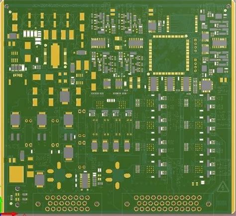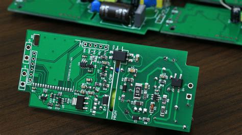
High frequency board pcb
Design Considerations For High Frequency PCB Boards
When designing high frequency printed circuit boards (PCBs), several critical considerations must be taken into account to ensure optimal performance and reliability. High frequency PCBs are integral to applications such as telecommunications, radar systems, and advanced computing, where signal integrity and minimal loss are paramount. As frequencies increase, the challenges associated with PCB design become more pronounced, necessitating a comprehensive understanding of various design elements.
To begin with, material selection is a fundamental aspect of high frequency PCB design.
The dielectric material used in the PCB substrate significantly influences signal propagation and loss. Materials such as PTFE (polytetrafluoroethylene) and ceramic-filled laminates are often preferred due to their low dielectric constant and minimal loss tangent. These properties help maintain signal integrity by reducing signal attenuation and dispersion. Moreover, the thermal stability of the material is crucial, as high frequency applications often generate substantial heat, which can affect performance and reliability.
In addition to material considerations, the layout of the PCB plays a pivotal role in high frequency applications.
The trace geometry, including width, spacing, and thickness, must be meticulously designed to minimize impedance discontinuities. Impedance control is essential to prevent signal reflections, which can degrade signal quality. Microstrip and stripline configurations are commonly employed to achieve controlled impedance, with careful attention paid to the dielectric height and trace dimensions. Furthermore, the use of ground planes is vital in providing a return path for signals, thereby reducing electromagnetic interference (EMI) and crosstalk between adjacent traces.
Transitioning to the topic of signal integrity, it is imperative to address the impact of vias and connectors on high frequency PCBs.
Vias, which are used to connect different layers of a PCB, can introduce inductance and capacitance, potentially leading to signal degradation. To mitigate these effects, designers often employ techniques such as back-drilling to remove unused via stubs, thereby reducing parasitic inductance. Similarly, the choice of connectors must be made with care, ensuring they are capable of handling the desired frequency range without introducing significant loss or reflection.
Moreover, power integrity is another critical consideration in high frequency PCB design.
Ensuring a stable power supply to all components is essential to prevent voltage fluctuations that can affect signal performance. This can be achieved through the use of decoupling capacitors strategically placed near power pins, as well as the implementation of power and ground planes to provide low impedance paths for current flow.
Thermal management is also a key factor in the design of high frequency PCBs.
As frequencies increase, so does the power dissipation, which can lead to elevated temperatures and potential component failure. Effective thermal management strategies, such as the use of heat sinks, thermal vias, and conductive cooling materials, are necessary to maintain the operational integrity of the PCB.
In conclusion, designing high frequency PCBs requires a holistic approach that encompasses material selection, layout optimization, signal and power integrity, and thermal management. By carefully considering these factors, designers can create PCBs that not only meet the demanding requirements of high frequency applications but also ensure long-term reliability and performance. As technology continues to advance, the importance of meticulous high frequency PCB design will only grow, underscoring the need for ongoing research and innovation in this critical field.
Material Selection For High Frequency PCB Applications
In the realm of high-frequency printed circuit boards (PCBs), material selection plays a pivotal role in determining the performance and reliability of the final product. As electronic devices continue to evolve, demanding faster speeds and higher frequencies, the need for specialized materials becomes increasingly critical. The choice of substrate material can significantly impact signal integrity, thermal management, and overall system efficiency, making it a crucial consideration for engineers and designers.
To begin with, one of the primary factors influencing material selection is the dielectric constant (Dk).
This parameter affects the speed at which signals propagate through the PCB. Materials with a low dielectric constant are generally preferred for high-frequency applications as they allow for faster signal transmission and reduced signal loss. Common materials such as FR-4, while cost-effective, may not always meet the stringent requirements of high-frequency applications due to their relatively high Dk values. Instead, materials like PTFE (polytetrafluoroethylene) and ceramics are often chosen for their superior electrical properties.
In addition to the dielectric constant, the dissipation factor (Df) is another critical parameter.
The dissipation factor measures the energy loss as heat within the material, which can lead to signal attenuation. For high-frequency applications, materials with a low dissipation factor are essential to minimize energy loss and maintain signal integrity. PTFE-based laminates, for instance, are known for their low Df values, making them suitable for applications where minimal signal loss is paramount.
Moreover, thermal management is a significant concern in high-frequency PCB design.
As frequencies increase, so does the potential for heat generation, which can adversely affect the performance and longevity of the PCB. Therefore, materials with good thermal conductivity are often sought after to efficiently dissipate heat. Ceramics and certain metal-backed laminates offer excellent thermal properties, providing a balance between electrical performance and heat management.
Furthermore, the coefficient of thermal expansion (CTE) is an important consideration, particularly in applications involving temperature fluctuations.
A mismatch in CTE between the substrate material and other components can lead to mechanical stress and potential failure. Selecting materials with a CTE that closely matches that of the components can mitigate these risks, ensuring the structural integrity of the PCB over its operational lifespan.
Additionally, manufacturability and cost are practical considerations that cannot be overlooked. While advanced materials like PTFE and ceramics offer superior performance, they can be more challenging to process and may incur higher costs. Engineers must weigh these factors against the performance benefits to determine the most suitable material for their specific application.
In conclusion, the selection of materials for high-frequency PCB applications is a complex process that requires careful consideration of various electrical, thermal, and mechanical properties. By understanding the implications of dielectric constant, dissipation factor, thermal conductivity, and coefficient of thermal expansion, engineers can make informed decisions that optimize the performance and reliability of their designs. As technology continues to advance, the demand for high-performance materials will only grow, underscoring the importance of material selection in the development of cutting-edge electronic devices.

Challenges In Manufacturing High Frequency PCBs
The manufacturing of high-frequency printed circuit boards (PCBs) presents a unique set of challenges that distinguish it from the production of standard PCBs. As electronic devices continue to evolve, the demand for high-frequency PCBs has surged, driven by applications in telecommunications, aerospace, and advanced computing. These PCBs are designed to operate at frequencies typically above 1 GHz, which necessitates a meticulous approach to their design and fabrication.
One of the primary challenges in manufacturing high-frequency PCBs is the selection of suitable materials.
Unlike conventional PCBs, which often use FR-4 as a substrate, high-frequency PCBs require materials with low dielectric constants and low loss tangents to minimize signal loss and ensure signal integrity. Materials such as PTFE (polytetrafluoroethylene) and ceramics are commonly used, but they come with their own set of difficulties. For instance, PTFE is known for its excellent electrical properties but poses challenges in terms of mechanical stability and adhesion, requiring specialized processing techniques.
In addition to material selection, the precision of the manufacturing process is crucial.
High-frequency signals are highly susceptible to interference and loss, which means that even minor deviations in the manufacturing process can lead to significant performance issues. This necessitates stringent control over the etching process to ensure that the copper traces are of the correct width and spacing. Moreover, the surface finish of the PCB must be carefully managed to prevent signal degradation. Techniques such as immersion silver or gold plating are often employed to achieve the desired surface characteristics.
Another significant challenge is the thermal management of high-frequency PCBs.
As the frequency of operation increases, so does the heat generated by the components. Effective thermal management is essential to maintain the reliability and performance of the PCB. This often involves the integration of thermal vias, heat sinks, and other cooling mechanisms into the design. However, these additions must be carefully balanced with the electrical requirements of the board to avoid introducing additional signal loss or interference.
Furthermore, the miniaturization of electronic components adds another layer of complexity to the manufacturing process.
As devices become smaller, the PCBs must also shrink, which requires more precise manufacturing techniques and equipment. The need for miniaturization often leads to the use of multilayer PCBs, which can complicate the manufacturing process due to the increased number of layers and the need for precise alignment and registration.
Testing and quality assurance are also critical components of the manufacturing process for high-frequency PCBs.
Given the complexity and precision required, thorough testing is essential to ensure that the final product meets the necessary performance standards. This often involves advanced testing techniques such as time-domain reflectometry and network analysis to verify the electrical characteristics of the board.
In conclusion, the manufacturing of high-frequency PCBs is a complex process that requires careful consideration of materials, precision in manufacturing, effective thermal management, and rigorous testing. As technology continues to advance, the demand for these specialized PCBs is likely to grow, necessitating ongoing innovation and adaptation in manufacturing techniques to meet the evolving needs of the industry.
Signal Integrity In High Frequency PCB Design
In the realm of high-frequency printed circuit board (PCB) design, signal integrity emerges as a pivotal concern, demanding meticulous attention to detail and a profound understanding of electromagnetic principles. As electronic devices continue to evolve, operating at increasingly higher frequencies, the challenges associated with maintaining signal integrity become more pronounced. This necessitates a comprehensive approach to PCB design, where every aspect, from material selection to layout configuration, plays a crucial role in ensuring optimal performance.
To begin with, the choice of substrate material is fundamental in high-frequency PCB design.
Materials such as FR-4, commonly used in lower frequency applications, may not suffice due to their higher dielectric losses at elevated frequencies. Instead, designers often opt for materials like Rogers or Teflon, which offer lower dielectric constants and reduced loss tangents. These materials help minimize signal attenuation and phase distortion, thereby preserving signal integrity across the board.
Moreover, the layout of a high-frequency PCB is another critical factor that influences signal integrity.
The arrangement of traces, vias, and components must be carefully orchestrated to mitigate issues such as crosstalk, reflection, and electromagnetic interference (EMI). For instance, maintaining consistent trace impedance is essential to prevent signal reflections that can degrade signal quality. This is typically achieved through controlled impedance design, where trace width, spacing, and the dielectric properties of the substrate are precisely calculated to match the characteristic impedance of the transmission line.
In addition to controlled impedance, the implementation of proper grounding techniques is vital in high-frequency PCB design.
A well-designed ground plane can significantly reduce EMI and improve signal return paths, thereby enhancing overall signal integrity. Designers often employ strategies such as stitching vias and ground fills to create a robust grounding network that minimizes potential interference and signal degradation.
Furthermore, the integration of differential signaling is a common practice in high-frequency PCB design to combat noise and improve signal integrity.
Differential pairs, which consist of two complementary signals, are less susceptible to external noise and crosstalk compared to single-ended signals. By routing these pairs closely together and ensuring equal electrical lengths, designers can achieve superior noise immunity and signal fidelity.
Transitioning to the realm of simulation and testing, these tools are indispensable in the pursuit of signal integrity in high-frequency PCB design.
Advanced simulation software allows designers to model and analyze the electromagnetic behavior of their designs before physical prototyping. This predictive capability enables the identification and resolution of potential signal integrity issues early in the design process, saving both time and resources. Once the PCB is fabricated, rigorous testing, including time-domain reflectometry (TDR) and vector network analysis, is conducted to validate the design and ensure compliance with performance specifications.
In conclusion, maintaining signal integrity in high-frequency PCB design is a multifaceted challenge that requires a holistic approach encompassing material selection, layout design, grounding strategies, and advanced simulation and testing. As technology continues to push the boundaries of frequency and performance, the principles of signal integrity will remain at the forefront of PCB design, guiding engineers in their quest to deliver reliable and efficient electronic solutions. Through a combination of theoretical knowledge and practical expertise, designers can navigate the complexities of high-frequency PCB design and achieve the desired outcomes in their projects.