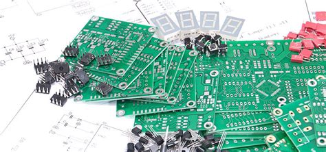
High frequency design pcb
Understanding Signal Integrity in High Frequency PCB Design
In the realm of high frequency printed circuit board (PCB) design, understanding signal integrity is paramount to ensuring optimal performance and reliability of electronic devices.
As technology advances, the demand for faster and more efficient electronic systems has led to the proliferation of high frequency applications, making signal integrity a critical consideration for engineers and designers.
Signal integrity refers to the quality and reliability of electrical signals as they travel through a PCB, and it is influenced by various factors including impedance, crosstalk, and electromagnetic interference (EMI).
To begin with, impedance control is a fundamental aspect of maintaining signal integrity in high frequency PCB design.
Impedance is the measure of opposition that a circuit presents to the flow of alternating current, and it is crucial to match the impedance of transmission lines to the source and load to minimize signal reflections. Mismatched impedance can lead to signal distortion, increased noise, and potential data loss. Therefore, designers must carefully calculate and control the impedance of traces, taking into account factors such as trace width, thickness, and the dielectric properties of the substrate material.
In addition to impedance control, crosstalk is another significant concern in high frequency PCB design.
Crosstalk occurs when a signal transmitted on one trace inadvertently induces a signal on an adjacent trace, leading to potential interference and degradation of signal quality. To mitigate crosstalk, designers can employ strategies such as increasing the spacing between traces, using ground planes to provide shielding, and routing critical signals on separate layers. These techniques help to isolate signals and reduce the likelihood of unwanted interactions.
Moreover, electromagnetic interference (EMI) poses a considerable challenge in maintaining signal integrity.
EMI can originate from both internal and external sources, and it can disrupt the normal operation of electronic circuits. To combat EMI, designers can implement various shielding techniques, such as using ground planes and metal enclosures, to protect sensitive components from external electromagnetic fields. Additionally, careful layout and routing practices, such as minimizing loop areas and avoiding sharp corners, can help reduce the emission and susceptibility of PCBs to EMI.
Furthermore, the choice of materials plays a crucial role in high frequency PCB design.
The dielectric constant and loss tangent of the substrate material can significantly impact signal propagation and attenuation. Low-loss materials are preferred for high frequency applications as they minimize signal degradation and ensure efficient transmission. Additionally, the use of advanced materials, such as high-frequency laminates, can further enhance signal integrity by providing better thermal stability and reduced dielectric losses.
In conclusion, understanding and addressing signal integrity issues is essential for successful high frequency PCB design.
By carefully controlling impedance, minimizing crosstalk, mitigating EMI, and selecting appropriate materials, designers can ensure that their PCBs deliver reliable and high-performance results. As the demand for high frequency applications continues to grow, the importance of signal integrity in PCB design will only become more pronounced. Therefore, staying informed about the latest techniques and best practices in signal integrity is crucial for engineers and designers striving to meet the challenges of modern electronic systems.

Techniques for Minimizing Electromagnetic Interference in High Frequency PCBs
In the realm of high frequency printed circuit board (PCB) design, minimizing electromagnetic interference (EMI) is a critical challenge that engineers must address to ensure optimal performance and reliability. As electronic devices become more complex and operate at higher frequencies, the potential for EMI increases, necessitating the implementation of effective design techniques.
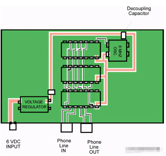
One fundamental approach to mitigating EMI in high frequency PCBs is through careful layout design.
By strategically placing components and routing traces, designers can significantly reduce the potential for interference. For instance, maintaining short and direct signal paths minimizes the loop area, thereby reducing the antenna effect that can lead to EMI. Additionally, separating high-speed signals from low-speed ones and keeping power and ground planes close together can further diminish interference.
Moreover, the use of proper grounding techniques is paramount in high frequency PCB design.
A solid ground plane acts as a reference point for signals and provides a low-impedance path for return currents, which is essential for minimizing EMI. Ensuring that the ground plane is continuous and unbroken helps prevent the formation of ground loops, which can be a significant source of interference. Furthermore, employing a multi-layer PCB design can enhance EMI performance by allowing for dedicated ground and power planes, thus improving signal integrity and reducing crosstalk between adjacent traces.
In addition to layout and grounding considerations, the selection of materials plays a crucial role in minimizing EMI.
High frequency PCBs often require substrates with low dielectric constants and low loss tangents to ensure signal integrity and reduce signal attenuation. Materials such as PTFE (polytetrafluoroethylene) and ceramic-filled laminates are commonly used in high frequency applications due to their favorable electrical properties. By choosing the appropriate materials, designers can enhance the overall performance of the PCB and mitigate potential EMI issues.
Another effective technique for reducing EMI is the implementation of proper shielding.
Shielding can be achieved through the use of metal enclosures or by incorporating shielding layers within the PCB itself. These shields act as barriers that prevent electromagnetic fields from radiating out of or into the PCB, thereby protecting sensitive components and reducing interference. Additionally, the use of ferrite beads and common-mode chokes can help suppress high-frequency noise on power and signal lines, further contributing to EMI reduction.
Furthermore, the integration of filtering components is essential in high frequency PCB design.
Filters, such as low-pass, high-pass, and band-pass filters, can be used to attenuate unwanted frequencies and prevent them from affecting the desired signals. By carefully designing and placing these filters, engineers can effectively control the frequency spectrum and minimize EMI.
Finally, simulation and testing are indispensable in the process of minimizing EMI in high frequency PCBs.
Advanced simulation tools allow designers to model and predict the electromagnetic behavior of their designs, enabling them to identify potential sources of interference and make necessary adjustments before physical prototyping. Once the PCB is fabricated, thorough testing using spectrum analyzers and other diagnostic equipment is crucial to ensure that the design meets the required EMI standards and performs as intended.
In conclusion, minimizing electromagnetic interference in high frequency PCBs requires a comprehensive approach that encompasses layout design, grounding techniques, material selection, shielding, filtering, and rigorous testing. By employing these strategies, engineers can effectively address the challenges posed by EMI and ensure the reliable operation of high frequency electronic devices.
Material Selection for Optimal Performance in High Frequency PCB Design
In the realm of high frequency printed circuit board (PCB) design, material selection plays a pivotal role in determining the overall performance and reliability of the final product. As electronic devices continue to evolve, operating at increasingly higher frequencies, the demand for PCBs that can effectively manage these frequencies without signal degradation has become more pronounced. Consequently, understanding the properties and implications of various materials is essential for engineers and designers aiming to optimize their high frequency PCB designs.
To begin with, one of the most critical factors to consider in material selection is the dielectric constant (Dk).
The dielectric constant of a material affects the speed at which an electrical signal can travel through the PCB. Materials with a lower dielectric constant are generally preferred for high frequency applications because they allow signals to propagate faster, reducing signal loss and improving overall performance. Furthermore, consistency in the dielectric constant across the material is crucial, as variations can lead to signal distortion and impedance mismatches, which are detrimental to high frequency operations.
In addition to the dielectric constant, the dissipation factor (Df) is another key parameter that influences material selection.
The dissipation factor measures the dielectric losses within the material, which can lead to signal attenuation. For high frequency applications, materials with a low dissipation factor are desirable as they minimize energy loss, thereby preserving signal integrity. This is particularly important in applications such as RF and microwave communications, where maintaining signal strength is paramount.
Moreover, thermal management is a significant consideration in high frequency PCB design.
As frequencies increase, so does the potential for heat generation, which can adversely affect the performance and longevity of the PCB. Therefore, selecting materials with good thermal conductivity is essential to efficiently dissipate heat and maintain the stability of the circuit. Materials such as ceramics and certain advanced composites offer excellent thermal properties, making them suitable candidates for high frequency applications.
Another aspect to consider is the material’s mechanical properties, including its ability to withstand environmental stresses such as temperature fluctuations and mechanical vibrations.
High frequency PCBs are often used in demanding environments, and the chosen material must be robust enough to maintain its structural integrity under such conditions. This ensures that the PCB remains reliable over its intended lifespan, reducing the risk of failure and the associated costs of repairs or replacements.
Furthermore, the compatibility of the material with the manufacturing process is an important consideration.
Some high performance materials may require specialized fabrication techniques, which can increase production costs and complexity. Therefore, it is essential to balance performance requirements with manufacturability to achieve a cost-effective solution.
In conclusion, selecting the appropriate material for high frequency PCB design is a multifaceted decision that requires careful consideration of various electrical, thermal, mechanical, and manufacturing factors. By understanding the implications of each material property and how they interact with the specific requirements of the application, designers can make informed choices that enhance the performance and reliability of their high frequency PCBs. As technology continues to advance, ongoing research and development in material science will undoubtedly yield new options, further expanding the possibilities for high frequency PCB design.
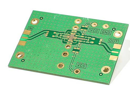
Advanced Routing Strategies for High Frequency PCB Layouts
In the realm of high frequency design, printed circuit board (PCB) layouts present unique challenges that require advanced routing strategies to ensure optimal performance. As electronic devices continue to evolve, operating at higher frequencies and faster speeds, the demand for precise and efficient PCB designs has never been more critical. High frequency PCBs are integral to applications such as telecommunications, radar systems, and high-speed computing, where signal integrity and minimal interference are paramount.
To begin with, understanding the fundamental principles of high frequency PCB design is essential.
At high frequencies, the behavior of electrical signals deviates significantly from that at lower frequencies. This is primarily due to the increased sensitivity to parasitic elements such as capacitance and inductance, which can lead to signal degradation. Therefore, one of the primary considerations in high frequency PCB design is the minimization of these parasitic effects. This can be achieved through careful component placement and routing strategies that prioritize short and direct signal paths.
Moreover, the choice of materials plays a crucial role in high frequency PCB design.
Materials with low dielectric constants and low loss tangents are preferred, as they help reduce signal loss and maintain signal integrity. Additionally, the use of controlled impedance traces is vital. Controlled impedance ensures that the characteristic impedance of the transmission lines matches the source and load, thereby minimizing reflections and signal distortion. This is particularly important in high frequency applications where even minor impedance mismatches can lead to significant performance issues.
Transitioning to routing strategies, one effective approach is the use of microstrip and stripline configurations.
Microstrip lines, which are traces on the outer layers of the PCB, are advantageous for their simplicity and ease of access. However, they are more susceptible to electromagnetic interference (EMI). On the other hand, stripline configurations, which are sandwiched between dielectric layers, offer better shielding from EMI but are more complex to implement. The choice between these configurations depends on the specific requirements of the application, including the frequency range and environmental conditions.
Furthermore, maintaining consistent trace widths and spacing is critical in high frequency PCB layouts.
Variations in trace width can lead to impedance discontinuities, which in turn cause signal reflections. To mitigate this, designers often employ differential pair routing for high-speed signals. Differential pairs consist of two traces carrying equal and opposite signals, which helps cancel out noise and reduce EMI. This technique is particularly effective in maintaining signal integrity over long distances.
In addition to these strategies, the use of ground planes is indispensable in high frequency PCB design.
Ground planes provide a return path for signals, reducing loop inductance and enhancing signal integrity. They also serve as a shield against EMI, further protecting sensitive components. It is important to ensure that ground planes are continuous and free of gaps, as discontinuities can lead to increased inductance and potential signal degradation.
Finally, simulation and testing are integral components of the high frequency PCB design process.
Advanced simulation tools allow designers to model and analyze the behavior of the PCB under various conditions, identifying potential issues before physical prototyping. This not only saves time and resources but also ensures that the final design meets the stringent requirements of high frequency applications.
In conclusion, advanced routing strategies for high frequency PCB layouts are essential for achieving optimal performance in modern electronic devices. By carefully considering factors such as material selection, impedance control, and routing configurations, designers can effectively address the challenges posed by high frequency applications, ensuring reliable and efficient operation.