High frequency pcb laminate
Understanding The Basics Of High Frequency PCB Laminate
High frequency PCB laminate is a critical component in the design and manufacturing of printed circuit boards (PCBs) that operate at high frequencies. As electronic devices become more sophisticated and demand for faster data transmission increases, the need for materials that can support high-frequency signals without significant loss or interference has become paramount. Understanding the basics of high frequency PCB laminate involves exploring its composition, properties, and applications, which are essential for engineers and designers working in the field of electronics.
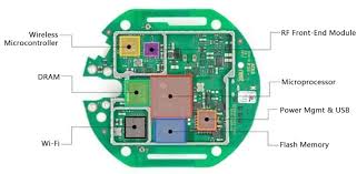
To begin with, high frequency PCB laminates are specialized materials used to fabricate PCBs that handle signals typically above 1 GHz.
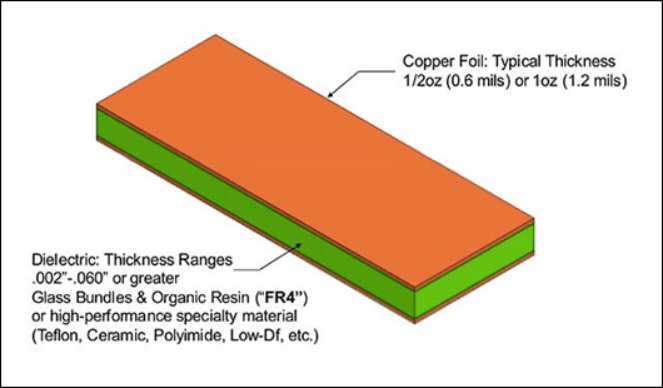
These laminates are distinct from standard FR-4 materials, which are commonly used in lower frequency applications. The primary difference lies in the dielectric properties of the materials. High frequency laminates are designed to have low dielectric constant (Dk) and low dissipation factor (Df), which are crucial for minimizing signal loss and ensuring signal integrity at high frequencies. Materials such as PTFE (polytetrafluoroethylene), ceramic-filled composites, and hydrocarbon-based laminates are often used due to their superior electrical performance.
Moreover, the choice of high frequency PCB laminate is influenced by several factors, including the specific frequency range, thermal management requirements, and mechanical properties.
For instance, PTFE-based laminates are known for their excellent electrical properties and are often used in microwave and RF applications. However, they can be challenging to process due to their softness and require specialized fabrication techniques. On the other hand, ceramic-filled laminates offer a good balance between performance and manufacturability, making them suitable for a wide range of high-frequency applications.
In addition to electrical properties, thermal management is a critical consideration when selecting high frequency PCB laminates.
As devices operate at higher frequencies, they tend to generate more heat, which can affect performance and reliability. Therefore, laminates with good thermal conductivity and stability are preferred to ensure efficient heat dissipation and maintain the integrity of the circuit. This is particularly important in applications such as radar systems, satellite communications, and high-speed data networks, where performance and reliability are paramount.
Furthermore, the mechanical properties of high frequency PCB laminates also play a significant role in their selection.
Factors such as dimensional stability, moisture absorption, and resistance to environmental conditions must be considered to ensure the longevity and durability of the PCB. For example, laminates with low moisture absorption are essential in applications where the PCB may be exposed to humid environments, as moisture can affect the dielectric properties and lead to signal degradation.
In conclusion, understanding the basics of high frequency PCB laminate is essential for designing and manufacturing PCBs that meet the demands of modern high-frequency applications. By considering the electrical, thermal, and mechanical properties of these laminates, engineers and designers can select the appropriate materials to ensure optimal performance and reliability. As technology continues to advance and the demand for high-speed data transmission grows, the importance of high frequency PCB laminates will only increase, making it a vital area of focus for the electronics industry.

Key Benefits Of Using High Frequency PCB Laminate In Modern Electronics
High frequency PCB laminate has become an essential component in the design and manufacture of modern electronic devices, offering a range of benefits that enhance performance, reliability, and efficiency. As the demand for faster and more efficient electronic devices continues to grow, the importance of selecting the right materials for printed circuit boards (PCBs) cannot be overstated. High frequency PCB laminates are specifically engineered to meet the needs of high-speed and high-frequency applications, making them indispensable in the development of advanced technologies.
One of the primary benefits of using high frequency PCB laminate is its ability to support high-speed signal transmission.
In today’s fast-paced digital world, the need for rapid data transfer is paramount. High frequency laminates are designed to minimize signal loss and distortion, ensuring that data is transmitted quickly and accurately. This is particularly important in applications such as telecommunications, where even the slightest delay or error can have significant consequences. By providing a stable and reliable platform for high-speed signals, these laminates help maintain the integrity of the data being transmitted.
In addition to supporting high-speed signal transmission, high frequency PCB laminates also offer excellent thermal management properties.
As electronic devices become more powerful, they generate more heat, which can lead to performance issues and even damage if not properly managed. High frequency laminates are designed to dissipate heat efficiently, helping to keep devices cool and functioning optimally. This is especially crucial in applications such as aerospace and automotive electronics, where reliability and performance are critical.
Moreover, high frequency PCB laminates exhibit superior electrical properties, which contribute to their effectiveness in modern electronics.
These laminates have low dielectric constants and low dissipation factors, which help reduce signal loss and improve overall performance. The low dielectric constant ensures that the signal speed is maximized, while the low dissipation factor minimizes energy loss as the signal travels through the circuit. This combination of properties makes high frequency laminates ideal for use in high-performance applications, such as radar systems and satellite communications.
Another significant advantage of high frequency PCB laminates is their ability to support miniaturization.
As electronic devices become smaller and more compact, the need for materials that can accommodate this trend is increasingly important. High frequency laminates are available in thin and lightweight forms, making them suitable for use in compact devices without compromising performance. This is particularly beneficial in the development of wearable technology and portable electronic devices, where space and weight are at a premium.
Furthermore, high frequency PCB laminates are known for their durability and reliability.
They are designed to withstand harsh environmental conditions, such as extreme temperatures and humidity, making them suitable for use in a wide range of applications. This durability ensures that devices remain operational and reliable over extended periods, reducing the need for frequent maintenance and replacement.
In conclusion, the use of high frequency PCB laminate in modern electronics offers numerous benefits that enhance the performance, reliability, and efficiency of electronic devices. By supporting high-speed signal transmission, providing excellent thermal management, exhibiting superior electrical properties, enabling miniaturization, and ensuring durability, these laminates play a crucial role in the advancement of technology. As the demand for faster, more efficient, and more compact electronic devices continues to grow, the importance of high frequency PCB laminates will only increase, solidifying their place as a key component in the future of electronics.
Challenges And Solutions In Designing With High Frequency PCB Laminate
Designing with high frequency PCB laminate presents a unique set of challenges that require careful consideration and innovative solutions. As electronic devices continue to evolve, the demand for high-speed communication and data processing has increased, necessitating the use of high frequency laminates in printed circuit boards (PCBs). These materials are essential for applications such as telecommunications, radar systems, and advanced computing, where signal integrity and performance are paramount. However, the transition to high frequency PCB laminates is not without its difficulties.
One of the primary challenges in working with high frequency laminates is managing signal integrity.
At high frequencies, even minor imperfections in the PCB design can lead to significant signal loss or distortion. This is due to the increased sensitivity of high frequency signals to parasitic capacitance, inductance, and electromagnetic interference. To mitigate these issues, designers must employ meticulous layout strategies, such as controlled impedance routing and the use of ground planes, to ensure that signals are transmitted with minimal degradation.
Moreover, the choice of laminate material itself is critical.
High frequency applications often require materials with low dielectric constants and low loss tangents to minimize signal attenuation. However, these materials can be more expensive and difficult to work with compared to traditional FR-4 laminates. Designers must balance performance requirements with cost considerations, often necessitating a thorough evaluation of different materials to find the optimal solution for a given application.
Thermal management is another significant challenge when designing with high frequency PCB laminates.
High frequency circuits can generate substantial heat, which, if not properly managed, can lead to component failure and reduced reliability. Effective thermal management strategies, such as the use of thermal vias, heat sinks, and appropriate laminate materials with good thermal conductivity, are essential to dissipate heat efficiently and maintain the performance and longevity of the PCB.
Additionally, manufacturing high frequency PCBs requires precision and expertise.
The fabrication process must accommodate the specific properties of high frequency laminates, which can be more sensitive to variations in temperature and pressure during manufacturing. This necessitates close collaboration with experienced PCB manufacturers who understand the nuances of working with these materials and can ensure that the final product meets the stringent requirements of high frequency applications.
Despite these challenges, there are several solutions that designers can employ to overcome the obstacles associated with high frequency PCB laminates.
Advanced simulation tools can be used to model and predict the behavior of high frequency circuits, allowing designers to identify potential issues and optimize their designs before fabrication. Furthermore, ongoing advancements in laminate materials and manufacturing techniques continue to expand the possibilities for high frequency PCB design, offering improved performance and reliability.
In conclusion, while designing with high frequency PCB laminate presents a range of challenges, these can be effectively addressed through careful planning, material selection, and collaboration with experienced manufacturers. By leveraging advanced design tools and staying abreast of technological developments, designers can create high-performance PCBs that meet the demanding requirements of modern high frequency applications. As the demand for faster and more efficient electronic devices continues to grow, the ability to successfully navigate the complexities of high frequency PCB design will remain a critical skill for engineers and designers in the field.

Comparing High Frequency PCB Laminate Materials: A Comprehensive Guide
In the realm of modern electronics, the demand for high-frequency printed circuit boards (PCBs) has surged, driven by the proliferation of advanced communication systems, radar technologies, and high-speed digital applications. At the heart of these high-frequency PCBs lies the choice of laminate material, which plays a pivotal role in determining the performance, reliability, and cost-effectiveness of the final product. As engineers and designers navigate the complexities of selecting the appropriate laminate, understanding the nuances of different materials becomes essential.
To begin with, high-frequency PCB laminates are specifically engineered to handle the rapid signal transitions and high-speed data rates characteristic of modern electronic applications.
These laminates are distinguished by their dielectric properties, thermal stability, and mechanical robustness. Among the most commonly used materials are PTFE (Polytetrafluoroethylene), ceramic-filled laminates, and hydrocarbon-based laminates. Each of these materials offers unique advantages and challenges, making the selection process a critical step in PCB design.
PTFE laminates, often recognized by the brand name Teflon, are renowned for their excellent dielectric properties and low loss tangent, making them ideal for microwave and RF applications. Their ability to maintain signal integrity at high frequencies is unparalleled, which is why they are frequently employed in aerospace and defense industries. However, PTFE laminates can be challenging to process due to their inherent flexibility and require specialized fabrication techniques. This can lead to increased manufacturing costs, which must be weighed against their performance benefits.
In contrast, ceramic-filled laminates offer a balance between performance and manufacturability.
By incorporating ceramic particles into the resin matrix, these laminates achieve a higher thermal conductivity and improved dimensional stability compared to pure PTFE materials. This makes them suitable for applications where thermal management is a concern, such as in power amplifiers and high-power RF circuits. Additionally, ceramic-filled laminates are generally easier to process than PTFE, which can result in cost savings during production. However, designers must consider the potential trade-offs in terms of dielectric constant variability and mechanical brittleness.
Hydrocarbon-based laminates present another viable option, particularly for applications requiring a cost-effective solution without compromising on performance.
These materials are engineered to mimic the dielectric properties of PTFE while offering improved mechanical strength and ease of processing. As a result, hydrocarbon-based laminates are often used in commercial telecommunications and automotive radar systems. While they may not match the ultra-low loss characteristics of PTFE, their affordability and versatility make them an attractive choice for many high-frequency applications.
As the demand for high-frequency PCBs continues to grow, the landscape of laminate materials is evolving, with manufacturers constantly innovating to meet the needs of the industry. Emerging materials, such as liquid crystal polymer (LCP) laminates, are gaining attention for their unique combination of low moisture absorption, excellent thermal stability, and high-frequency performance. These advancements promise to expand the options available to designers, enabling even greater optimization of PCB performance.
In conclusion, selecting the right high-frequency PCB laminate material involves a careful consideration of various factors, including dielectric properties, thermal management, mechanical strength, and cost. By understanding the characteristics and trade-offs of different materials, engineers can make informed decisions that align with the specific requirements of their applications. As technology continues to advance, the ongoing development of innovative laminate materials will undoubtedly play a crucial role in shaping the future of high-frequency electronics.