High frequency pcb manufacturing
Challenges In High Frequency PCB Design
High frequency PCB (Printed Circuit Board) design presents a unique set of challenges that require careful consideration and expertise. As electronic devices become more sophisticated and demand higher performance, the need for high frequency PCBs has grown significantly. These PCBs are essential in applications such as telecommunications, aerospace, and advanced computing, where they facilitate the rapid transmission of signals. However, designing these boards is not without its difficulties, and understanding these challenges is crucial for engineers and manufacturers alike.
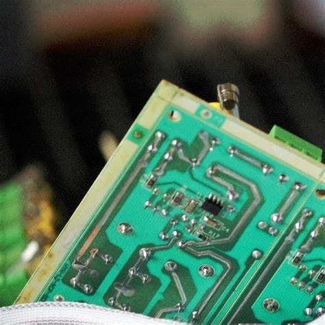
One of the primary challenges in high frequency PCB design is signal integrity.
At high frequencies, even minor imperfections in the PCB layout can lead to significant signal degradation. This is because high frequency signals are more susceptible to interference and loss, which can result in signal distortion or attenuation. To mitigate these issues, designers must pay close attention to the layout of traces, ensuring that they are as short and direct as possible. Additionally, the use of controlled impedance traces is often necessary to maintain signal integrity, requiring precise calculations and careful material selection.
Another significant challenge is managing electromagnetic interference (EMI).
High frequency signals can generate electromagnetic fields that interfere with other components on the board or with external devices. This interference can lead to malfunction or reduced performance of the electronic system. To address this, designers must implement effective shielding and grounding techniques. This often involves the use of ground planes and careful placement of components to minimize the potential for EMI. Moreover, the choice of materials with appropriate dielectric properties is crucial in reducing electromagnetic interference.
Thermal management also poses a challenge in high frequency PCB design.
As the frequency of operation increases, so does the power consumption, leading to higher heat generation. Excessive heat can adversely affect the performance and reliability of the PCB, potentially causing component failure. Therefore, effective thermal management strategies are essential. This may include the use of thermal vias, heat sinks, and advanced cooling techniques to dissipate heat efficiently. Additionally, selecting materials with high thermal conductivity can help in managing heat more effectively.
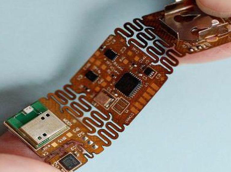
Furthermore, the miniaturization of electronic devices adds another layer of complexity to high frequency PCB design.
As devices become smaller, the available space for PCB components is reduced, necessitating more compact and efficient designs. This requires innovative approaches to component placement and routing, often involving multi-layer PCBs to accommodate the necessary circuitry within a limited area. The challenge lies in maintaining performance while adhering to size constraints, which demands a high level of precision and expertise.
In addition to these technical challenges, high frequency PCB design is also constrained by cost considerations.
The materials and processes required for high frequency applications are often more expensive than those used in standard PCBs. This includes specialized substrates, advanced fabrication techniques, and rigorous testing procedures to ensure performance and reliability. Balancing these costs with the need for high performance is a critical aspect of the design process.
In conclusion, high frequency PCB design is a complex and demanding field that requires a deep understanding of various technical and practical challenges. From ensuring signal integrity and managing electromagnetic interference to addressing thermal issues and accommodating miniaturization, each aspect demands careful attention and expertise. As technology continues to advance, the importance of overcoming these challenges will only grow, underscoring the need for continued innovation and development in high frequency PCB manufacturing.

Material Selection For High Frequency PCBs
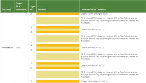
In the realm of high frequency PCB manufacturing, the selection of materials plays a pivotal role in determining the performance and reliability of the final product. As electronic devices continue to evolve, demanding faster speeds and higher frequencies, the need for specialized materials becomes increasingly critical. High frequency PCBs are typically used in applications such as telecommunications, radar systems, and advanced computing, where signal integrity and minimal loss are paramount. Therefore, understanding the properties and implications of various materials is essential for engineers and manufacturers alike.
To begin with, one must consider the dielectric constant (Dk) of the material, which significantly influences the speed at which signals can travel through the PCB.
Materials with a low dielectric constant are preferred for high frequency applications as they allow signals to propagate faster, reducing the potential for signal distortion. Common materials such as FR-4, while cost-effective, may not always meet the stringent requirements of high frequency applications due to their relatively high dielectric constant. Instead, materials like PTFE (Polytetrafluoroethylene), ceramics, and certain advanced composites are often chosen for their superior electrical properties.
In addition to the dielectric constant, the dissipation factor (Df) is another critical parameter to consider.
The dissipation factor measures the inherent energy loss within the material as the signal passes through it. A lower dissipation factor indicates that less energy is lost as heat, which is crucial for maintaining signal integrity at high frequencies. Materials such as Rogers laminates are renowned for their low dissipation factors, making them a popular choice in high frequency PCB manufacturing.
Moreover, thermal management is a key consideration in material selection.
High frequency PCBs often operate in environments where heat dissipation is a concern. Therefore, materials with good thermal conductivity are essential to prevent overheating and ensure the longevity of the PCB. Advanced materials that combine low dielectric constants with high thermal conductivity are particularly advantageous, as they address both electrical and thermal performance requirements.
Furthermore, the mechanical properties of the material cannot be overlooked.
High frequency PCBs may be subjected to various environmental stresses, including temperature fluctuations and mechanical vibrations. Therefore, materials that offer a good balance of flexibility and rigidity are preferred to withstand these conditions without compromising performance. PTFE-based materials, for instance, provide excellent mechanical stability while maintaining the necessary electrical properties.
Transitioning to the manufacturing process, it is important to note that the choice of material also impacts the fabrication techniques employed.
Some high frequency materials may require specialized handling and processing, which can influence the overall cost and complexity of production. Therefore, manufacturers must weigh the benefits of advanced materials against the potential challenges they present in the manufacturing process.
In conclusion, the selection of materials for high frequency PCB manufacturing is a multifaceted decision that requires careful consideration of electrical, thermal, and mechanical properties. By understanding the unique requirements of high frequency applications and the characteristics of available materials, engineers can make informed choices that enhance the performance and reliability of their designs. As technology continues to advance, the development of new materials will undoubtedly play a crucial role in meeting the ever-increasing demands of high frequency applications.
Techniques For Minimizing Signal Loss In High Frequency PCBs
In the realm of high frequency printed circuit boards (PCBs), minimizing signal loss is a critical concern for engineers and manufacturers alike. As electronic devices become increasingly sophisticated, the demand for high frequency PCBs has surged, necessitating advanced techniques to ensure signal integrity. One of the primary strategies for minimizing signal loss involves the careful selection of materials. High frequency PCBs often utilize substrates with low dielectric constants and low loss tangents, such as PTFE (polytetrafluoroethylene) or ceramic-filled laminates. These materials are chosen for their ability to reduce dielectric losses, which are a significant source of signal attenuation at high frequencies.
In addition to material selection, the design of the PCB itself plays a crucial role in minimizing signal loss.
Engineers must pay close attention to the layout of traces, which are the conductive pathways that carry signals across the board. To reduce signal loss, traces should be kept as short as possible and should follow a direct path. This minimizes the resistance and inductance that can degrade signal quality. Furthermore, the width of the traces should be optimized to match the characteristic impedance of the transmission line, thereby reducing reflections and ensuring efficient signal transmission.
Another important technique involves the use of controlled impedance.
By designing traces with a specific impedance, engineers can ensure that the signal is transmitted with minimal reflection and loss. This is particularly important in high frequency applications where even small impedance mismatches can lead to significant signal degradation. Controlled impedance is achieved through careful consideration of trace width, spacing, and the dielectric properties of the substrate.
Moreover, the implementation of ground planes is a widely used technique to minimize signal loss in high frequency PCBs.
Ground planes provide a return path for signals, reducing electromagnetic interference (EMI) and crosstalk between adjacent traces. By placing a continuous ground plane beneath the signal traces, engineers can create a controlled environment that enhances signal integrity. This technique not only minimizes signal loss but also improves the overall performance of the PCB by reducing noise and enhancing thermal management.
Additionally, the use of via structures is another critical consideration in high frequency PCB design.
Vias, which are used to connect different layers of a PCB, can introduce parasitic inductance and capacitance, leading to signal loss. To mitigate these effects, engineers often employ techniques such as back-drilling, which removes unnecessary via stubs, thereby reducing signal reflections and improving high frequency performance.
Furthermore, surface finish selection is an often-overlooked aspect that can impact signal loss.
High frequency PCBs benefit from surface finishes that provide a smooth and uniform surface, such as immersion silver or electroless nickel immersion gold (ENIG). These finishes reduce surface roughness, which can otherwise increase signal attenuation at high frequencies.
In conclusion, minimizing signal loss in high frequency PCBs requires a multifaceted approach that encompasses material selection, trace design, controlled impedance, ground plane implementation, via optimization, and surface finish selection. By employing these techniques, engineers can enhance the performance and reliability of high frequency PCBs, meeting the demands of modern electronic applications. As technology continues to advance, the importance of these techniques will only grow, underscoring the need for ongoing innovation and precision in high frequency PCB manufacturing.
Innovations In High Frequency PCB Manufacturing Technology
In recent years, the field of high frequency PCB (Printed Circuit Board) manufacturing has witnessed significant advancements, driven by the increasing demand for faster and more efficient electronic devices. As technology continues to evolve, the need for PCBs that can support high-frequency signals without compromising performance has become paramount. This has led to a series of innovations aimed at enhancing the capabilities of high frequency PCBs, ensuring they meet the rigorous demands of modern applications.
One of the most notable innovations in high frequency PCB manufacturing is the development of advanced materials.
Traditional materials, such as FR-4, are often inadequate for high-frequency applications due to their dielectric properties. Consequently, manufacturers have turned to specialized materials like PTFE (Polytetrafluoroethylene) and ceramic-filled laminates, which offer superior electrical performance. These materials exhibit lower dielectric constants and loss tangents, which are crucial for minimizing signal loss and maintaining signal integrity at high frequencies. By utilizing these advanced materials, manufacturers can produce PCBs that are not only capable of handling high-frequency signals but also offer improved thermal management and mechanical stability.
In addition to material advancements, the precision of manufacturing processes has also seen significant improvements.
The miniaturization of electronic components and the increasing complexity of circuit designs necessitate highly accurate manufacturing techniques. Innovations such as laser direct imaging (LDI) and advanced photolithography have enabled manufacturers to achieve finer line widths and tighter tolerances. These techniques allow for the creation of intricate circuit patterns that are essential for high-frequency applications, where even the slightest deviation can lead to performance issues. Moreover, the use of automated optical inspection (AOI) systems ensures that any defects are detected early in the manufacturing process, thereby enhancing the overall quality and reliability of the PCBs.
Furthermore, the integration of simulation and modeling tools has revolutionized the design phase of high frequency PCB manufacturing.
Engineers can now utilize sophisticated software to simulate the electrical behavior of their designs before they are physically produced. This capability allows for the optimization of circuit layouts, ensuring that potential issues such as crosstalk and electromagnetic interference (EMI) are addressed proactively. By identifying and mitigating these challenges during the design phase, manufacturers can significantly reduce the risk of costly redesigns and production delays.
Another critical innovation is the adoption of advanced surface finish technologies.
High frequency PCBs often require specific surface finishes to ensure optimal signal transmission and longevity. Techniques such as electroless nickel immersion gold (ENIG) and immersion silver have gained popularity due to their ability to provide excellent conductivity and corrosion resistance. These finishes not only enhance the electrical performance of the PCBs but also contribute to their durability, making them suitable for a wide range of high-frequency applications.
As the demand for high-frequency electronic devices continues to grow, the importance of innovations in PCB manufacturing cannot be overstated. The advancements in materials, manufacturing precision, design simulation, and surface finishes collectively contribute to the production of high-performance PCBs that meet the stringent requirements of modern technology. By embracing these innovations, manufacturers are well-equipped to support the ever-evolving landscape of high-frequency applications, ensuring that electronic devices can operate at peak efficiency and reliability.