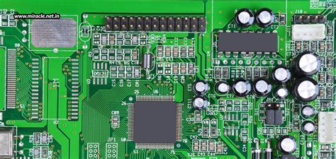
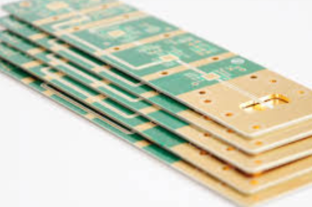
High-frequency pcb trace
Designing High-Frequency PCB Traces for Optimal Signal Integrity
Designing high-frequency PCB traces for optimal signal integrity is a critical aspect of modern electronics engineering. As the demand for faster and more efficient electronic devices continues to grow, the need for precise and reliable high-frequency PCB design becomes increasingly important. High-frequency signals, typically defined as those above 100 MHz, present unique challenges that must be addressed to ensure the integrity and performance of the final product.
One of the primary considerations in high-frequency PCB design is the impedance control of the traces.
Impedance, which is the resistance to the flow of alternating current, must be carefully managed to prevent signal reflections and loss. This is achieved by designing traces with consistent width and spacing, as well as by selecting appropriate materials for the PCB substrate. The dielectric constant of the substrate material plays a significant role in determining the impedance of the traces. Therefore, choosing a material with a stable and low dielectric constant is essential for maintaining signal integrity.
In addition to impedance control, minimizing signal loss is another crucial factor in high-frequency PCB design.
Signal loss can occur due to various factors, including the resistance of the traces, dielectric losses in the substrate material, and radiation losses. To mitigate these losses, designers often use wider traces and thicker copper layers. Furthermore, the use of low-loss dielectric materials can significantly reduce dielectric losses, thereby preserving signal strength over longer distances.
Another important aspect of high-frequency PCB design is the management of crosstalk, which is the unwanted coupling of signals between adjacent traces.
Crosstalk can lead to signal degradation and interference, particularly in densely packed PCBs. To minimize crosstalk, designers should maintain adequate spacing between high-frequency traces and use ground planes to provide a return path for the signals. Additionally, differential signaling, which involves using pairs of traces to carry complementary signals, can help reduce crosstalk and improve signal integrity.
The layout of the PCB also plays a vital role in ensuring optimal signal integrity.
High-frequency signals are more susceptible to electromagnetic interference (EMI) and radiation, which can be exacerbated by poor layout practices. To mitigate these issues, designers should avoid sharp bends and abrupt changes in trace width, as these can cause signal reflections and radiation. Instead, smooth curves and gradual transitions should be used. Moreover, placing high-frequency components and traces away from noisy power and ground planes can help reduce EMI and improve overall performance.
Thermal management is another critical consideration in high-frequency PCB design.
High-frequency signals can generate significant heat, which can affect the performance and reliability of the PCB. Effective thermal management strategies, such as the use of thermal vias, heat sinks, and proper component placement, are essential to dissipate heat and maintain the integrity of the high-frequency signals.
In conclusion, designing high-frequency PCB traces for optimal signal integrity requires careful consideration of various factors, including impedance control, signal loss, crosstalk management, layout practices, and thermal management. By addressing these challenges, designers can ensure that their high-frequency PCBs deliver reliable and efficient performance, meeting the demands of modern electronic devices. As technology continues to advance, the importance of precise and effective high-frequency PCB design will only grow, making it a critical area of focus for electronics engineers.
Material Selection for High-Frequency PCB Traces
When designing high-frequency printed circuit boards (PCBs), the selection of materials for the traces is a critical factor that significantly influences the performance and reliability of the final product. High-frequency signals, typically defined as those operating above 100 MHz, are particularly sensitive to the properties of the materials used in the PCB. Therefore, understanding the key material characteristics and their impact on signal integrity is essential for engineers and designers.
One of the primary considerations in material selection for high-frequency PCB traces is the dielectric constant (Dk) of the substrate material.
The dielectric constant affects the signal propagation speed and impedance of the traces. Materials with a low and stable dielectric constant are preferred because they minimize signal distortion and ensure consistent impedance, which is crucial for maintaining signal integrity at high frequencies. Common materials with favorable dielectric properties include PTFE (polytetrafluoroethylene), also known as Teflon, and certain ceramic-filled laminates. These materials offer low dielectric constants and low loss tangents, making them suitable for high-frequency applications.
In addition to the dielectric constant, the loss tangent or dissipation factor (Df) of the substrate material is another important parameter.
The loss tangent measures the amount of signal loss due to the dielectric material itself. A lower loss tangent indicates less signal attenuation, which is particularly important for high-frequency signals that can degrade quickly over distance. Materials such as Rogers RO3000 and RO4000 series laminates are often chosen for their low loss tangents, which help maintain signal strength and integrity over longer trace lengths.
The thermal properties of the substrate material also play a significant role in high-frequency PCB design.
High-frequency circuits can generate substantial heat, and materials with poor thermal management can lead to performance degradation or even failure. Therefore, materials with good thermal conductivity and stability are essential. For instance, ceramic-filled PTFE laminates not only offer excellent dielectric properties but also provide superior thermal performance, making them ideal for high-frequency applications that require efficient heat dissipation.
Moreover, the surface roughness of the copper traces is a critical factor that can affect signal integrity at high frequencies.
A smoother copper surface reduces skin effect losses, where high-frequency currents tend to flow on the surface of the conductor, leading to increased resistance and signal loss. Advanced fabrication techniques, such as using low-profile copper foils, can help achieve smoother surfaces and improve high-frequency performance.
Another consideration is the coefficient of thermal expansion (CTE) of the substrate material.
A low and matched CTE between the substrate and the copper traces ensures mechanical stability and reduces the risk of delamination or cracking during thermal cycling. Materials like PTFE composites and certain high-performance epoxy resins offer low CTE values, making them suitable for high-frequency applications that may experience varying thermal conditions.
Furthermore, the choice of materials must also take into account the manufacturability and cost-effectiveness of the PCB. .
While high-performance materials like PTFE and ceramic-filled laminates offer excellent electrical and thermal properties, they can be more challenging to process and more expensive than standard FR-4 materials. Therefore, a balance must be struck between performance requirements and practical considerations such as ease of fabrication and budget constraints.
In conclusion, selecting the appropriate materials for high-frequency PCB traces involves a careful evaluation of dielectric properties, thermal performance, surface roughness, and mechanical stability. By understanding and optimizing these factors, designers can ensure that their high-frequency circuits achieve the desired performance and reliability, ultimately leading to successful and efficient electronic products.
Techniques to Minimize Crosstalk in High-Frequency PCB Traces
In the realm of high-frequency printed circuit boards (PCBs), crosstalk is a significant concern that can degrade signal integrity and overall system performance. Crosstalk occurs when a signal transmitted on one trace inadvertently affects another nearby trace, leading to unwanted interference. To mitigate this issue, several techniques can be employed to minimize crosstalk in high-frequency PCB traces, ensuring optimal functionality and reliability of the electronic system.
One of the primary methods to reduce crosstalk is to maintain adequate spacing between adjacent traces.
By increasing the distance between traces, the electromagnetic coupling that causes crosstalk is diminished. This approach is particularly effective in high-frequency applications where the wavelength of the signals is relatively short. Additionally, employing differential signaling can further mitigate crosstalk. Differential pairs, which consist of two complementary signals, are less susceptible to external noise and interference, as the noise tends to affect both signals equally, allowing the differential receiver to cancel out the common-mode noise.
Another crucial technique involves the use of ground planes.
Ground planes act as a reference point for signals and provide a low-impedance path for return currents. By placing a continuous ground plane adjacent to signal layers, the loop area for the return current is minimized, thereby reducing the potential for crosstalk. Moreover, incorporating ground vias at regular intervals along the signal traces can enhance the effectiveness of the ground plane, ensuring a consistent return path and further mitigating crosstalk.
Shielding is another effective strategy to combat crosstalk in high-frequency PCB traces.
By enclosing sensitive traces within a grounded shield, the electromagnetic interference from adjacent traces is significantly reduced. This can be achieved through the use of guard traces, which are grounded traces placed between signal traces to act as a barrier against crosstalk. Additionally, employing coaxial cables or twisted-pair cables for critical signal paths can provide superior shielding and further minimize crosstalk.
The layout of the PCB also plays a pivotal role in minimizing crosstalk.
Careful consideration of trace routing can help avoid parallel runs of high-frequency signals, which are more prone to crosstalk. Instead, traces should be routed orthogonally or at angles to each other to reduce the coupling effect. Furthermore, maintaining a consistent trace width and avoiding abrupt changes in trace geometry can help maintain signal integrity and reduce crosstalk.
In addition to physical layout considerations, the choice of materials can impact crosstalk.
High-frequency PCBs often utilize low-loss dielectric materials with controlled impedance characteristics. These materials help maintain signal integrity by reducing signal attenuation and minimizing the potential for crosstalk. Moreover, selecting materials with low dielectric constant and low dissipation factor can further enhance the performance of high-frequency traces.
Finally, signal integrity analysis and simulation tools can be invaluable in identifying and mitigating crosstalk issues during the design phase.
By simulating the PCB layout and analyzing the signal behavior, potential crosstalk hotspots can be identified and addressed before the physical prototype is manufactured. This proactive approach can save time and resources by ensuring that the final design meets the required performance specifications.
In conclusion, minimizing crosstalk in high-frequency PCB traces is essential for maintaining signal integrity and ensuring the reliable operation of electronic systems. By employing techniques such as adequate trace spacing, differential signaling, ground planes, shielding, careful layout, and appropriate material selection, designers can effectively mitigate crosstalk and enhance the performance of high-frequency PCBs. Additionally, leveraging signal integrity analysis tools can provide valuable insights and help optimize the design for minimal crosstalk, ultimately leading to more robust and reliable electronic systems.
The Role of Impedance Control in High-Frequency PCB Trace Design
In the realm of high-frequency printed circuit board (PCB) design, the role of impedance control cannot be overstated. As electronic devices continue to evolve, operating at increasingly higher frequencies, the need for precise impedance control becomes paramount. This necessity stems from the fact that high-frequency signals are particularly susceptible to various forms of signal degradation, including reflection, crosstalk, and electromagnetic interference (EMI). Consequently, ensuring that PCB traces maintain a consistent impedance is crucial for preserving signal integrity and overall device performance.
To understand the importance of impedance control, it is essential to first grasp the concept of impedance itself.
Impedance, in the context of PCB traces, is the measure of opposition that a circuit presents to the flow of alternating current (AC) at a given frequency. It is a complex quantity, comprising both resistance and reactance, and is typically expressed in ohms. In high-frequency applications, the impedance of a PCB trace is influenced by several factors, including the trace width, thickness, length, and the dielectric properties of the substrate material. Variations in any of these parameters can lead to impedance mismatches, which in turn can cause signal reflections and distortions.
One of the primary methods for achieving impedance control in high-frequency PCB design is through the use of controlled impedance traces.
These traces are designed with specific dimensions and materials to ensure that their impedance remains within a desired range. For instance, microstrip and stripline configurations are commonly employed to achieve controlled impedance. A microstrip trace is a conductor situated on the surface of a dielectric substrate, with a ground plane located on the opposite side. In contrast, a stripline trace is sandwiched between two ground planes within the substrate. Both configurations allow for precise control over the trace impedance by adjusting parameters such as trace width, substrate thickness, and dielectric constant.
Moreover, the choice of substrate material plays a critical role in impedance control.
High-frequency PCBs often utilize materials with low dielectric constants and low loss tangents to minimize signal attenuation and dispersion. Common materials include polytetrafluoroethylene (PTFE), also known as Teflon, and various ceramic-filled laminates. These materials offer superior electrical properties compared to traditional FR-4 substrates, making them ideal for high-frequency applications.
In addition to material selection and trace configuration, advanced simulation and modeling tools are indispensable for achieving accurate impedance control.
These tools enable designers to predict the impedance characteristics of PCB traces and make necessary adjustments before fabrication. By simulating the electromagnetic behavior of the traces, designers can identify potential issues and optimize the layout to ensure consistent impedance across the entire PCB.
Furthermore, manufacturing tolerances must be carefully managed to maintain impedance control.
Variations in etching processes, substrate thickness, and dielectric properties can all impact the final impedance of the traces. Therefore, close collaboration between PCB designers and manufacturers is essential to ensure that the fabricated boards meet the specified impedance requirements.
In conclusion, impedance control is a critical aspect of high-frequency PCB trace design, directly impacting signal integrity and device performance. By employing controlled impedance traces, selecting appropriate substrate materials, utilizing advanced simulation tools, and managing manufacturing tolerances, designers can effectively mitigate the challenges associated with high-frequency signal transmission. As electronic devices continue to push the boundaries of speed and functionality, the importance of precise impedance control in PCB design will only continue to grow.