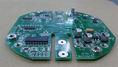
High frequency rogers ceramic pcb
Best Practices For High Frequency Signal PCB Layout
Designing printed circuit boards (PCBs) for high-frequency signals requires meticulous attention to detail and adherence to best practices to ensure optimal performance. High-frequency signals, typically those above 50 MHz, are particularly susceptible to various forms of interference and signal degradation. Therefore, implementing best practices in PCB layout is crucial to maintaining signal integrity and minimizing issues such as crosstalk, electromagnetic interference (EMI), and signal reflection.
One of the fundamental principles in high-frequency PCB design is the careful management of trace impedance.
Impedance control is essential because mismatched impedance can lead to signal reflections, which degrade signal quality. To achieve consistent impedance, designers should use controlled impedance traces, which involve precise calculations of trace width, spacing, and the dielectric properties of the PCB material. Utilizing simulation tools can aid in predicting and verifying the impedance of traces before manufacturing.
In addition to impedance control, minimizing the length of high-frequency signal traces is another critical practice.
Longer traces act as antennas, increasing the likelihood of EMI and signal loss. Therefore, keeping traces as short as possible helps to reduce these risks. When longer traces are unavoidable, using differential pairs can be beneficial. Differential signaling involves two complementary signals traveling together, which helps to cancel out noise and reduce EMI.
Ground planes play a pivotal role in high-frequency PCB design.
A continuous ground plane provides a low-impedance return path for signals, which is essential for maintaining signal integrity. It also helps to shield sensitive signals from external noise. Designers should avoid splitting ground planes, as this can create impedance discontinuities and increase the risk of signal degradation. Instead, maintaining a solid, unbroken ground plane beneath high-frequency traces is recommended.
Another best practice is the careful placement of decoupling capacitors.
These capacitors help to filter out high-frequency noise and provide a stable power supply to active components. Placing decoupling capacitors as close as possible to the power pins of integrated circuits (ICs) is crucial for their effectiveness. Additionally, using multiple capacitors with different values can help to filter a broader range of frequencies.
Signal integrity can also be enhanced by using proper termination techniques.
Termination resistors, placed at the end of signal traces, help to match the impedance of the trace to the load, thereby reducing reflections. Series termination, where a resistor is placed in series with the signal trace near the driver, is another effective method for improving signal integrity.
Routing high-frequency signals on inner layers of a multi-layer PCB can provide additional shielding from external noise.
When routing on outer layers is necessary, using ground fills or guard traces adjacent to high-frequency traces can help to mitigate EMI. Guard traces are grounded traces placed parallel to signal traces, which help to absorb and redirect noise away from the signal path.
Finally, maintaining proper spacing between high-frequency traces is essential to prevent crosstalk.
Crosstalk occurs when signals on adjacent traces interfere with each other, leading to signal degradation. Adhering to the recommended spacing guidelines based on the operating frequency and signal amplitude can significantly reduce the risk of crosstalk.
In conclusion, designing PCBs for high-frequency signals demands a comprehensive understanding of various factors that influence signal integrity. By implementing best practices such as impedance control, minimizing trace lengths, maintaining continuous ground planes, strategically placing decoupling capacitors, using proper termination techniques, routing on inner layers, and ensuring adequate trace spacing, designers can effectively mitigate potential issues and achieve reliable, high-performance PCB layouts.
Material Selection For High Frequency PCB Design
When designing printed circuit boards (PCBs) for high-frequency applications, the selection of materials becomes a critical factor that can significantly influence the performance and reliability of the final product. High-frequency signals, typically those above 1 GHz, demand materials with specific electrical properties to ensure signal integrity and minimize losses. Consequently, understanding the key attributes of various materials and their impact on high-frequency signal propagation is essential for any PCB designer.
To begin with, the dielectric constant (Dk) of the substrate material is a primary consideration.
The dielectric constant affects the speed at which signals travel through the PCB and can influence impedance control. Materials with a low and stable dielectric constant are preferred for high-frequency applications because they help maintain signal integrity and reduce signal distortion. Common materials such as FR-4, which is widely used in standard PCB designs, may not be suitable for high-frequency applications due to its relatively high and variable dielectric constant. Instead, materials like Rogers RO4000 series, which offer a low and stable dielectric constant, are often chosen for high-frequency designs.
In addition to the dielectric constant, the dissipation factor (Df) is another crucial parameter.
The dissipation factor measures the dielectric losses within the material, which can lead to signal attenuation and power loss. For high-frequency applications, materials with a low dissipation factor are essential to minimize these losses and ensure efficient signal transmission. High-performance materials such as PTFE (Polytetrafluoroethylene) composites, which exhibit low dissipation factors, are frequently used in high-frequency PCB designs.
Thermal management is another important aspect to consider when selecting materials for high-frequency PCBs.
High-frequency signals can generate significant heat, and the chosen material must be able to dissipate this heat effectively to prevent thermal-related failures. Materials with high thermal conductivity, such as ceramic-filled PTFE composites, can help manage heat dissipation and maintain the reliability of the PCB under high-frequency operation.
Moreover, the coefficient of thermal expansion (CTE) is a vital factor in material selection.
The CTE measures how much a material expands or contracts with temperature changes. A mismatch in CTE between the substrate material and other components, such as copper traces, can lead to mechanical stress and potential failure of the PCB. Therefore, selecting materials with a CTE that closely matches that of copper is crucial for maintaining the structural integrity of the PCB in high-frequency applications.
Furthermore, surface finish plays a significant role in high-frequency PCB design.
The choice of surface finish can impact signal loss and overall performance. For instance, Electroless Nickel Immersion Gold (ENIG) is a popular surface finish due to its excellent conductivity and smooth surface, which helps reduce signal loss at high frequencies. However, other finishes like immersion silver or immersion tin may also be considered based on specific application requirements.
In conclusion, the selection of materials for high-frequency PCB design involves a careful evaluation of several key parameters, including dielectric constant, dissipation factor, thermal management, coefficient of thermal expansion, and surface finish. By understanding and optimizing these factors, designers can ensure that their high-frequency PCBs deliver superior performance, reliability, and efficiency. As high-frequency applications continue to evolve, staying informed about advancements in material technology will be essential for meeting the ever-increasing demands of modern electronic systems.
Managing Signal Integrity In High Frequency PCBs
Managing signal integrity in high-frequency PCBs is a critical aspect of modern electronic design, as the performance and reliability of these circuits depend heavily on maintaining the integrity of the signals they carry. As frequencies increase, the challenges associated with signal integrity become more pronounced, necessitating a comprehensive understanding of various factors that can affect signal quality.
One of the primary considerations in high-frequency PCB design is the choice of materials.
The dielectric properties of the substrate material can significantly influence signal propagation. Materials with low dielectric constants and low loss tangents are preferred, as they minimize signal attenuation and dispersion. Additionally, the thickness of the dielectric layer and the copper trace width must be carefully controlled to ensure consistent impedance, which is crucial for maintaining signal integrity.
Another important factor is the layout of the PCB.
The placement and routing of traces must be meticulously planned to avoid issues such as crosstalk, reflections, and electromagnetic interference (EMI). To mitigate crosstalk, designers should maintain adequate spacing between high-frequency traces and use ground planes to provide a return path for signals, thereby reducing the potential for interference. Furthermore, differential signaling can be employed to enhance noise immunity and reduce EMI. Differential pairs should be routed together with consistent spacing and length to ensure that any noise affects both lines equally, allowing the receiver to cancel out the common-mode noise.
Signal reflections, which can cause significant degradation in high-frequency signals, are another critical concern.
These reflections occur when there is a mismatch in impedance along the signal path. To address this, impedance matching techniques must be employed. This involves designing traces with controlled impedance, which can be achieved by adjusting the trace width, spacing, and the dielectric properties of the substrate. Additionally, termination resistors can be used at the end of transmission lines to match the impedance and minimize reflections.
The power distribution network (PDN) also plays a vital role in maintaining signal integrity.
A well-designed PDN ensures that the power supply noise is minimized, which is essential for the proper functioning of high-frequency circuits. Decoupling capacitors should be strategically placed close to the power pins of integrated circuits to filter out high-frequency noise. Moreover, the use of multiple ground planes can help to reduce the loop inductance and provide a low-impedance path for return currents, further enhancing signal integrity.
Thermal management is another aspect that cannot be overlooked in high-frequency PCB design.
High-frequency circuits often generate significant amounts of heat, which can affect signal integrity and the overall performance of the PCB. Effective thermal management strategies, such as the use of thermal vias, heat sinks, and proper airflow, are essential to dissipate heat and maintain the reliability of the circuit.
In conclusion, managing signal integrity in high-frequency PCBs requires a holistic approach that encompasses material selection, meticulous layout planning, impedance matching, effective power distribution, and robust thermal management. By addressing these factors, designers can ensure that high-frequency signals are transmitted with minimal degradation, thereby enhancing the performance and reliability of modern electronic devices. As technology continues to advance and operating frequencies increase, the importance of maintaining signal integrity in PCB design will only become more critical, underscoring the need for ongoing research and development in this field.
Techniques For Reducing EMI In High Frequency PCB Designs
In the realm of high frequency signal PCB design, managing electromagnetic interference (EMI) is paramount to ensuring optimal performance and reliability. EMI can significantly degrade the functionality of electronic circuits, leading to signal integrity issues and potential system failures. Therefore, employing effective techniques to mitigate EMI is crucial for engineers working on high frequency PCB designs.
One fundamental technique for reducing EMI is the careful layout of the PCB.
Proper component placement and routing are essential to minimize the coupling of noise between different parts of the circuit. For instance, placing high-speed components close to each other and routing high-frequency signals away from sensitive analog components can significantly reduce EMI. Additionally, maintaining short and direct signal paths helps to minimize the loop area, thereby reducing the potential for radiated emissions.
Another critical aspect is the use of ground planes.
A continuous ground plane provides a low-impedance path for return currents, which helps to reduce the loop area and, consequently, the radiated EMI. It is advisable to use a multilayer PCB design, where one or more layers are dedicated to ground planes. This not only improves EMI performance but also enhances signal integrity by providing a stable reference plane for high-speed signals.
Moreover, decoupling capacitors play a vital role in mitigating EMI.
Placing these capacitors close to the power pins of integrated circuits helps to filter out high-frequency noise and provides a stable power supply. It is essential to use capacitors with low equivalent series resistance (ESR) and to select appropriate values to cover a wide frequency range. Additionally, using multiple capacitors in parallel can further improve the filtering effect.
Shielding is another effective technique for reducing EMI in high frequency PCB designs.
Enclosing sensitive components or entire sections of the PCB in a conductive shield can prevent external electromagnetic fields from interfering with the circuit. This is particularly important in environments with high levels of electromagnetic noise. However, it is crucial to ensure that the shield is properly grounded to avoid creating additional EMI issues.
Furthermore, differential signaling can be employed to reduce EMI.
By using differential pairs, where two complementary signals are transmitted together, the common-mode noise is canceled out, resulting in lower EMI. This technique is especially useful for high-speed data transmission, as it improves signal integrity and reduces susceptibility to external noise.
In addition to these techniques, careful consideration of the PCB materials is essential.
High-frequency signals are more susceptible to losses and dispersion, which can exacerbate EMI issues. Therefore, selecting materials with low dielectric constant and low loss tangent can help to maintain signal integrity and reduce EMI. Materials such as FR-4, while commonly used, may not always be suitable for very high-frequency applications, and alternatives like Rogers or Teflon-based laminates might be necessary.
Lastly, simulation and testing are indispensable in the design process.
Using electromagnetic simulation tools can help identify potential EMI issues early in the design phase, allowing for corrective measures to be implemented before fabrication. Additionally, thorough testing of the PCB in its intended operating environment is crucial to ensure that EMI levels are within acceptable limits.
In conclusion, reducing EMI in high frequency PCB designs requires a multifaceted approach, encompassing careful layout, the use of ground planes, decoupling capacitors, shielding, differential signaling, appropriate material selection, and rigorous simulation and testing. By employing these techniques, engineers can significantly enhance the performance and reliability of high frequency PCBs, ensuring they meet the stringent requirements of modern electronic systems.


