High-Layer Count PCB Manufacturing Process Guide
Introduction
Printed Circuit Boards (PCBs) are the backbone of modern electronics, enabling complex interconnections in devices ranging from consumer electronics to aerospace systems. As technology advances, the demand for high-layer count PCBs (typically 8 layers or more) has grown significantly. These PCBs are essential for high-speed digital circuits, RF applications, and high-power systems where signal integrity, thermal management, and space constraints are critical.
Manufacturing high-layer count PCBs presents unique challenges, including precise layer alignment, controlled impedance, and reliable via structures. This guide provides a comprehensive overview of the manufacturing process, key considerations, and best practices for producing high-quality, high-layer count PCBs.
1. Design Considerations for High-Layer Count PCBs
Before manufacturing begins, the PCB design must be optimized for manufacturability. Key design considerations include:
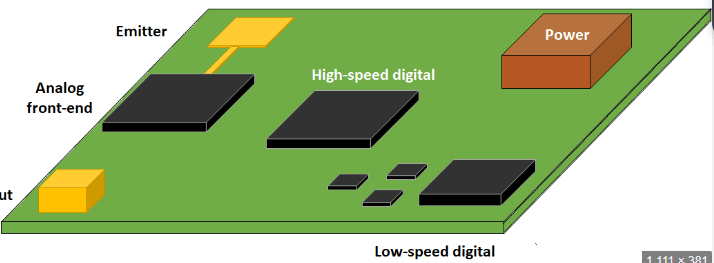
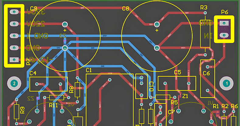
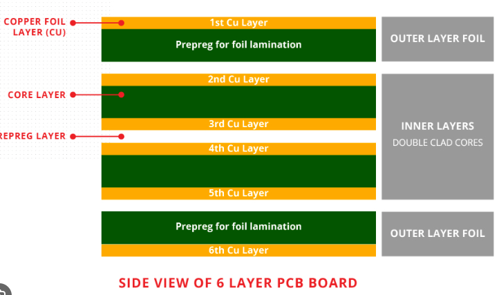
1.1 Layer Stackup Configuration
- Signal, Power, and Ground Layers: A well-planned stackup minimizes crosstalk and ensures proper impedance control.
- Symmetrical Construction: Prevents warping by balancing copper distribution and dielectric materials.
- Dielectric Material Selection: High-frequency applications may require low-loss materials like Rogers or Isola laminates.
1.2 Controlled Impedance
- Trace width and spacing must be calculated based on dielectric thickness and material properties.
- Differential pairs and high-speed signals require precise impedance matching (e.g., 50Ω single-ended, 100Ω differential).
1.3 Via Structures
- Through-Hole Vias: Standard for low-complexity boards but consume space.
- Blind and Buried Vias: Used in HDI (High-Density Interconnect) designs to save space.
- Microvias: Essential for ultra-high-density designs, often laser-drilled.
1.4 Thermal Management
- Thermal vias and copper pours help dissipate heat in high-power designs.
- Metal-core or insulated metal substrates may be used for extreme thermal requirements.
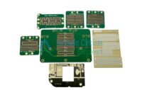
2. High-Layer Count PCB Manufacturing Process
The manufacturing process for high-layer count PCBs involves several critical steps:
2.1 Material Preparation
- Core and Prepreg Selection: FR-4 is common, but high-speed designs may require specialized materials.
- Copper Clad Laminates: Thin copper foils (e.g., ½ oz or 1 oz) are used for fine traces.
2.2 Inner Layer Imaging
- Cleaning: Remove contaminants from copper surfaces.
- Photoresist Application: A light-sensitive film is applied to the copper.
- Exposure: UV light transfers the circuit pattern from a photomask.
- Development: Unexposed photoresist is removed, leaving the desired circuit pattern.
- Etching: Chemical etching removes unwanted copper, leaving the traces.
- Stripping: The remaining photoresist is removed.
2.3 Automated Optical Inspection (AOI)
- Scans inner layers for defects like shorts, opens, or misalignments before lamination.
2.4 Layer Lamination
- Layers are stacked with prepreg (uncured epoxy resin) between them.
- The stack is placed in a lamination press under high temperature and pressure to bond layers.
2.5 Drilling
- Mechanical drilling creates through-holes for vias and component leads.
- Laser drilling is used for microvias in HDI designs.
2.6 Plating and Via Formation
- Electroless Copper Deposition: A thin conductive layer is applied to hole walls.
- Electroplating: Builds up copper thickness in holes and on surfaces.
- Via Filling: Conductive or non-conductive fill may be used for reliability.
2.7 Outer Layer Imaging and Etching
- Similar to inner layer imaging but performed on the outer layers after lamination.
2.8 Solder Mask Application
- A protective coating (usually green epoxy) is applied, leaving exposed pads for soldering.
- UV exposure and development define the solder mask pattern.
2.9 Surface Finish
- Common finishes include:
- HASL (Hot Air Solder Leveling): Traditional but not ideal for fine-pitch components.
- ENIG (Electroless Nickel Immersion Gold): Flat surface, good for soldering and wire bonding.
- OSP (Organic Solderability Preservative): Cost-effective but less durable.
- Immersion Silver/Tin: Alternative to ENIG for specific applications.
2.10 Electrical Testing
- Flying Probe Test: Checks for opens, shorts, and impedance issues.
- Bed of Nails Test: Used for high-volume production.
2.11 Final Inspection and Routing
- Visual and AOI Inspection: Ensures no physical defects.
- Routing (Depaneling): Individual PCBs are cut from the panel.
3. Key Challenges and Solutions
3.1 Layer Misalignment
- Solution: Use high-precision registration systems and laser direct imaging (LDI).
3.2 Signal Integrity Issues
- Solution: Careful stackup design, impedance control, and proper grounding.
3.3 Thermal Stress and Warping
- Solution: Symmetrical stackup, proper material selection, and controlled lamination process.
3.4 Via Reliability
- Solution: Use filled vias or cap plating for mechanical strength.
4. Best Practices for High-Layer Count PCB Manufacturing
- Collaborate Early with Fabricators: Ensure design for manufacturability (DFM) compliance.
- Use Advanced Simulation Tools: Predict signal integrity and thermal performance.
- Implement Rigorous Testing: Include impedance testing and thermal cycling.
- Choose Experienced Manufacturers: High-layer PCBs require specialized expertise.
Conclusion
High-layer count PCB manufacturing is a complex but essential process for advanced electronics. By following optimized design rules, precise fabrication techniques, and thorough testing, manufacturers can produce reliable, high-performance PCBs for demanding applications. As technology evolves, innovations in materials, laser drilling, and additive manufacturing will further enhance the capabilities of multilayer PCBs.
By adhering to this guide, engineers and manufacturers can navigate the challenges of high-layer count PCB production and achieve superior results.