High Precision ADC PCB Layout: Best Practices and Design Considerations
Introduction
High-precision analog-to-digital converters (ADCs) are critical components in applications such as medical instrumentation, industrial sensing, and high-fidelity data acquisition systems. However, achieving the full performance of a high-resolution ADC (e.g., 16-bit, 18-bit, or 24-bit) requires careful printed circuit board (PCB) layout. Poor layout practices can introduce noise, distortion, and signal integrity issues, degrading the ADC’s performance.
This article explores key considerations for designing a high-precision ADC PCB, including power supply routing, grounding strategies, signal integrity, and noise mitigation techniques.
1. Power Supply Design and Decoupling
1.1 Power Supply Noise Sensitivity
High-resolution ADCs are sensitive to power supply noise, which can introduce jitter, distortion, and reduced signal-to-noise ratio (SNR). Switching regulators, digital noise, and improper decoupling can all contribute to power-related errors.
1.2 Recommended Practices:
- Use Low-Noise Linear Regulators (LDOs): Switching regulators should be avoided near the ADC. Instead, use LDOs with low output noise (e.g., <10 µV RMS).
- Multi-Stage Filtering: Implement RC or LC filters to further reduce high-frequency noise.
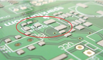
- Proper Decoupling:
- Place 0.1 µF ceramic capacitors close to the ADC power pins.
- Use bulk capacitors (10 µF to 100 µF) for low-frequency stability.
- For very high-resolution ADCs (>18 bits), consider tantalum or low-ESR polymer capacitors.
1.3 Power Plane Layout
- Dedicate separate power planes for analog (AVDD) and digital (DVDD) supplies.
- Avoid routing digital power traces near analog signals.
2. Grounding Strategies
2.1 Star Ground vs. Split Ground
- Star Ground: A single ground point minimizes ground loops but may not be practical for complex layouts.
- Split Ground (with Care): Separate analog and digital ground planes can reduce noise coupling, but they must be connected at a single point near the ADC.
2.2 Ground Plane Design
- Use a solid ground plane beneath the ADC and analog circuitry.
- Avoid splits or slots in the ground plane under sensitive analog traces.
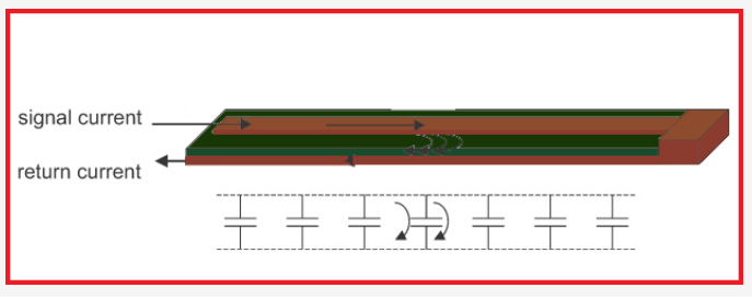
- Ensure low-impedance return paths for high-frequency signals.
2.3 ADC Ground Pins
- Connect the ADC’s AGND (Analog Ground) and DGND (Digital Ground) at the device (unless the datasheet specifies otherwise).
- Do not float any ground pins—always provide a low-impedance return path.
3. Signal Routing and Integrity
3.1 Analog Input Routing
- Minimize Trace Length: Keep analog input traces as short as possible to reduce noise pickup.
- Avoid Crosstalk: Separate analog inputs from digital signals (≥3x trace width spacing).
- Differential Pairs: For differential ADCs, maintain tight coupling and equal trace lengths to minimize skew.
3.2 Clock and Digital Signal Routing
- Clock Jitter Matters: A noisy clock degrades ADC performance. Use a low-jitter oscillator and route the clock away from analog signals.
- Buffered Clock Lines: If the clock travels a long distance, use a clock buffer to prevent degradation.
- Digital Output Isolation: Add series resistors (e.g., 22–100 Ω) on digital output lines to reduce ringing.
3.3 Shielding and Guard Rings
- Guard Rings: Surround sensitive analog traces with a grounded guard ring to reduce leakage currents.
- Shielding: In extremely noisy environments, consider shielded cables or a Faraday cage for critical analog sections.
4. Thermal and Mechanical Considerations
4.1 Thermal Management
- ADCs with high resolution (>18 bits) may be sensitive to temperature drift.
- Avoid placing heat-generating components (e.g., regulators, processors) near the ADC.
- Use thermal relief pads for soldering but ensure low thermal resistance for stability.
4.2 PCB Stackup
- 4-Layer PCB Recommended:
- Layer 1: Signal (analog & critical traces)
- Layer 2: Ground plane (solid)
- Layer 3: Power planes
- Layer 4: Digital signals (if needed)
- 6-Layer PCB for High-Speed ADCs: Additional ground/power planes improve noise immunity.
5. Testing and Validation
5.1 Noise Measurement
- Use a spectrum analyzer or oscilloscope with FFT to check for power supply noise and clock jitter.
- Evaluate SNR, THD (Total Harmonic Distortion), and ENOB (Effective Number of Bits).
5.2 Layout Review Checklist
- Are power and ground planes uninterrupted under the ADC?
- Are decoupling capacitors placed correctly (close to power pins)?
- Are analog and digital signals properly separated?
- Is the clock signal clean and free from excessive ringing?
Conclusion
Designing a high-precision ADC PCB requires meticulous attention to power integrity, grounding, signal routing, and noise control. By following best practices—such as proper decoupling, strategic ground plane design, and careful signal isolation—engineers can maximize ADC performance and achieve the full resolution specified in the datasheet.
For mission-critical applications, simulation tools (e.g., SPICE, HyperLynx) can further validate the design before fabrication. Always refer to the ADC manufacturer’s layout guidelines, as some high-resolution ADCs have specific requirements.
By adhering to these principles, designers can ensure stable, high-accuracy ADC performance in even the most demanding applications.