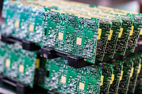
High speed chase pcb
Evolution Of High Speed Chase PCB Technology
The evolution of high-speed chase printed circuit board (PCB) technology has been a fascinating journey marked by significant advancements and innovations.
As electronic devices have become more complex and demand for faster processing speeds has increased, the need for high-speed PCBs has grown exponentially.
This evolution is driven by the relentless pursuit of efficiency, miniaturization, and enhanced performance in electronic systems.
Initially, PCBs were simple and primarily used for basic electronic applications. However, as technology advanced, the limitations of these early designs became apparent. The need for faster data transmission and higher processing speeds led to the development of high-speed PCBs. These advanced PCBs are designed to handle high-frequency signals and support the rapid data transfer required by modern electronic devices.
One of the key factors in the evolution of high-speed chase PCB technology is the development of new materials.
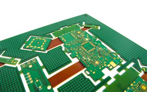
Traditional PCBs were made from materials like FR-4, which, while adequate for low-speed applications, were not suitable for high-speed data transmission.
To address this, manufacturers began experimenting with advanced materials such as polyimide, Teflon, and ceramic substrates.
These materials offer superior electrical properties, such as lower dielectric constants and reduced signal loss, which are crucial for high-speed applications.
In addition to material advancements, the design and layout of high-speed PCBs have also evolved significantly.
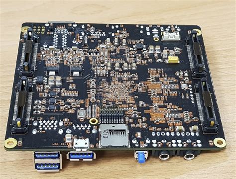
The complexity of modern electronic devices necessitates intricate PCB designs that can accommodate multiple layers and dense component placement. This has led to the development of multilayer PCBs, which allow for more compact and efficient designs. Furthermore, advanced design techniques, such as controlled impedance and differential pair routing, have been implemented to ensure signal integrity and minimize electromagnetic interference.
Another critical aspect of high-speed chase PCB technology is the integration of advanced simulation and testing tools.
As the complexity of PCBs has increased, so too has the need for accurate simulation and testing to ensure optimal performance. Modern design software now includes sophisticated simulation capabilities that allow engineers to model and analyze the behavior of high-speed signals within a PCB.
This enables the identification and mitigation of potential issues before the manufacturing process begins, reducing the risk of costly errors and rework.
Moreover, the manufacturing processes for high-speed PCBs have also seen significant advancements. Precision manufacturing techniques, such as laser drilling and advanced etching processes, have been developed to accommodate the intricate designs and tight tolerances required by high-speed applications. These techniques ensure that the final product meets the stringent performance requirements necessary for high-speed data transmission.
As we look to the future, the evolution of high-speed chase PCB technology shows no signs of slowing down.
The ongoing development of new materials, design techniques, and manufacturing processes will continue to push the boundaries of what is possible in electronic design. Additionally, the rise of emerging technologies, such as 5G and the Internet of Things (IoT), will further drive the demand for high-speed PCBs, as these applications require even faster data transmission and processing capabilities.
In conclusion, the evolution of high-speed chase PCB technology is a testament to the relentless pursuit of innovation in the electronics industry. Through advancements in materials, design, simulation, and manufacturing, high-speed PCBs have become an essential component of modern electronic devices, enabling faster and more efficient data processing. As technology continues to advance, the role of high-speed PCBs will only become more critical, paving the way for the next generation of electronic innovations.
Designing Efficient High-Speed Chase PCBs
Designing efficient high-speed chase printed circuit boards (PCBs) is a critical task that requires a deep understanding of both the theoretical and practical aspects of electronic design.
As technology continues to advance, the demand for faster and more reliable electronic devices has increased, making the design of high-speed PCBs more important than ever. To achieve optimal performance, designers must consider a variety of factors, including signal integrity, power distribution, and thermal management.
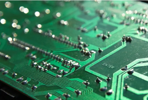
Signal integrity is a primary concern in high-speed PCB design.
As the speed of electronic signals increases, the potential for signal degradation also rises. This can lead to issues such as signal reflection, crosstalk, and electromagnetic interference (EMI), which can significantly impact the performance of the device.
To mitigate these issues, designers must carefully consider the layout of the PCB.
For instance, maintaining consistent impedance throughout the board is crucial. This can be achieved by using controlled impedance traces and ensuring that the trace width and spacing are appropriate for the signal frequency. Additionally, the use of differential signaling can help reduce EMI and improve signal integrity by minimizing the loop area through which the signal travels.
Power distribution is another critical aspect of high-speed PCB design.
As devices become more complex, the demand for power increases, necessitating efficient power distribution networks (PDNs). A well-designed PDN ensures that all components receive the necessary power without causing voltage drops or introducing noise into the system. To achieve this, designers often use a combination of power planes and decoupling capacitors.
Power planes provide a low-impedance path for current flow, while decoupling capacitors help filter out noise and stabilize the power supply.
Furthermore, careful placement of these components is essential to minimize inductance and resistance, which can adversely affect the performance of the PDN.
Thermal management is also a key consideration in high-speed PCB design.
As electronic components operate at higher speeds, they generate more heat, which can lead to thermal issues if not properly managed. Excessive heat can cause components to fail or degrade over time, reducing the overall reliability of the device.
To address this, designers must implement effective thermal management strategies. This may include the use of thermal vias, heat sinks, and thermal pads to dissipate heat away from critical components. Additionally, selecting materials with high thermal conductivity can help improve heat dissipation across the PCB.
In addition to these technical considerations, designers must also be mindful of manufacturing constraints and cost implications.
High-speed PCBs often require advanced fabrication techniques, such as microvias and high-density interconnects (HDIs), which can increase production costs. Therefore, it is important to balance performance requirements with budgetary constraints to ensure a cost-effective design.
In conclusion, designing efficient high-speed chase PCBs involves a comprehensive approach that addresses signal integrity, power distribution, and thermal management, while also considering manufacturing and cost factors. By carefully analyzing each of these elements and employing best practices, designers can create PCBs that meet the demands of modern high-speed electronic devices. As technology continues to evolve, staying informed about the latest advancements and techniques in PCB design will be essential for achieving success in this ever-changing field.

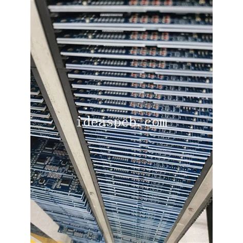
Challenges In High-Speed Chase PCB Manufacturing
In the realm of printed circuit board (PCB) manufacturing, the demand for high-speed chase PCBs has been steadily increasing, driven by the rapid advancements in technology and the need for faster, more efficient electronic devices.
However, the manufacturing of high-speed chase PCBs presents a unique set of challenges that manufacturers must navigate to meet the stringent requirements of modern electronics.
Understanding these challenges is crucial for ensuring the reliability and performance of the final product.
One of the primary challenges in high-speed chase PCB manufacturing is signal integrity. As electronic devices operate at higher frequencies, the potential for signal degradation increases. This degradation can result from various factors, including impedance mismatches, crosstalk, and electromagnetic interference.
To mitigate these issues, manufacturers must employ advanced design techniques and materials that can support high-frequency signals without compromising performance.
This often involves the use of specialized substrates and precise control over trace geometries to maintain consistent impedance throughout the board.
In addition to signal integrity, thermal management is another critical challenge in high-speed chase PCB manufacturing.
As devices become more powerful, they generate more heat, which can adversely affect performance and reliability. Effective thermal management solutions are essential to dissipate heat efficiently and prevent overheating.
This may involve the integration of thermal vias, heat sinks, or advanced cooling systems into the PCB design. Manufacturers must carefully consider the thermal properties of materials and the layout of components to ensure optimal heat dissipation.
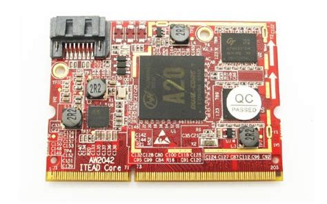
Moreover, the miniaturization of electronic components adds another layer of complexity to high-speed chase PCB manufacturing.
As devices become smaller and more compact, the need for densely packed PCBs increases. This requires manufacturers to adopt advanced fabrication techniques, such as microvia technology and high-density interconnects, to accommodate the reduced space while maintaining performance.
The precision required in these processes demands state-of-the-art equipment and meticulous attention to detail to avoid defects that could compromise the functionality of the PCB.
Furthermore, the choice of materials plays a pivotal role in overcoming the challenges associated with high-speed chase PCB manufacturing.
The materials used must possess excellent electrical properties, thermal stability, and mechanical strength to withstand the demands of high-speed applications. Manufacturers often turn to advanced materials like low-loss laminates and high-performance copper foils to achieve the desired performance characteristics. However, sourcing these materials can be challenging due to their cost and availability, necessitating strategic planning and supplier partnerships.
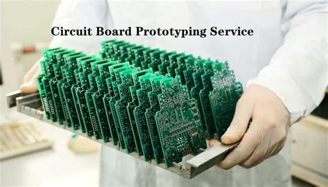
In addition to technical challenges, high-speed chase PCB manufacturing also faces economic and logistical hurdles.
The complexity of these PCBs often results in longer production times and higher costs, which can impact the overall profitability of manufacturing operations. To address these issues, manufacturers must optimize their production processes, invest in automation, and implement rigorous quality control measures to minimize waste and ensure consistent output.
In conclusion, the manufacturing of high-speed chase PCBs is fraught with challenges that require a multifaceted approach to overcome. From ensuring signal integrity and effective thermal management to navigating the intricacies of miniaturization and material selection, manufacturers must employ a combination of advanced technologies, innovative design strategies, and efficient production practices. By addressing these challenges head-on, manufacturers can produce high-speed chase PCBs that meet the demands of modern electronic devices, paving the way for continued technological advancement.
Future Trends In High-Speed Chase PCB Development
In recent years, the development of high-speed chase printed circuit boards (PCBs) has become a focal point in the electronics industry, driven by the increasing demand for faster and more efficient electronic devices.
As technology continues to advance at a rapid pace, the need for PCBs that can support high-speed data transmission without compromising performance or reliability is more critical than ever.
This evolution is not only reshaping the landscape of PCB design but also setting new standards for future innovations.
One of the primary trends in high-speed chase PCB development is the integration of advanced materials. Traditional materials such as FR-4 are gradually being supplemented or replaced by high-performance alternatives like polyimide, Rogers, and Teflon.
These materials offer superior dielectric properties, which are essential for minimizing signal loss and ensuring signal integrity at high frequencies.
As a result, they enable the design of PCBs that can handle the demands of modern high-speed applications, such as 5G networks, advanced computing systems, and high-frequency communication devices.
In addition to material advancements, the miniaturization of components is another significant trend influencing high-speed chase PCB development.
As electronic devices become smaller and more compact, the need for PCBs that can accommodate densely packed components without sacrificing performance is paramount.
This has led to the adoption of techniques such as microvia technology and high-density interconnect (HDI) designs.
These approaches allow for more efficient use of space on the PCB, enabling the integration of more components and the facilitation of faster data transmission.
Moreover, the increasing complexity of electronic systems necessitates the use of sophisticated design tools and simulation software.
These tools are crucial for predicting the behavior of high-speed signals and identifying potential issues such as crosstalk, electromagnetic interference (EMI), and signal reflection.
By leveraging advanced simulation capabilities, designers can optimize PCB layouts to ensure that they meet the stringent requirements of high-speed applications.
This not only enhances the performance of the final product but also reduces the time and cost associated with prototyping and testing.
Furthermore, the trend towards sustainability and environmental responsibility is also impacting high-speed chase PCB development.
Manufacturers are increasingly adopting eco-friendly practices, such as using lead-free solder and recyclable materials, to minimize the environmental impact of PCB production. This shift is driven by both regulatory requirements and consumer demand for greener products. As a result, the industry is seeing a rise in the development of PCBs that are not only high-performing but also environmentally sustainable.
Looking ahead, the future of high-speed chase PCB development is likely to be shaped by ongoing advancements in technology and materials science.
Innovations such as flexible and stretchable PCBs, which offer new possibilities for wearable technology and other emerging applications, are expected to gain traction.
Additionally, the integration of artificial intelligence and machine learning into PCB design processes holds the potential to further enhance the efficiency and effectiveness of high-speed PCB development.
In conclusion, the evolution of high-speed chase PCBs is a dynamic and multifaceted process, driven by the need for faster, more efficient, and environmentally sustainable electronic solutions. As the industry continues to innovate, the development of high-speed PCBs will undoubtedly play a pivotal role in shaping the future of electronics, paving the way for new applications and technologies that were once thought to be beyond reach.