High speed digital pcb
Designing High-Speed Digital PCBs: Best Practices and Techniques
Designing high-speed digital printed circuit boards (PCBs) requires a meticulous approach to ensure signal integrity, minimize electromagnetic interference (EMI), and achieve optimal performance. As digital systems operate at increasingly higher frequencies, the challenges associated with high-speed PCB design become more pronounced. Therefore, understanding and implementing best practices and techniques is crucial for engineers and designers.
To begin with, one of the fundamental aspects of high-speed PCB design is the careful consideration of signal integrity.
Signal integrity refers to the quality and reliability of electrical signals as they travel through the PCB. High-speed signals are susceptible to various forms of degradation, such as reflection, crosstalk, and attenuation. To mitigate these issues, it is essential to maintain controlled impedance throughout the signal paths. Controlled impedance can be achieved by designing transmission lines with consistent width and spacing, and by using appropriate materials with known dielectric properties.
Moreover, the layout of the PCB plays a significant role in ensuring signal integrity.
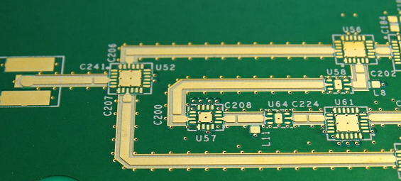
Proper placement of components and routing of traces can significantly reduce the risk of signal degradation. For instance, keeping high-speed signal traces as short as possible and avoiding sharp bends can help maintain signal quality. Additionally, differential pairs should be routed together with consistent spacing to minimize noise and crosstalk. It is also advisable to use ground planes and power planes to provide a low-impedance return path for high-speed signals, thereby reducing EMI.
Transitioning to the topic of power distribution, it is imperative to design an efficient power delivery network (PDN) for high-speed digital PCBs.
A well-designed PDN ensures that all components receive stable and clean power, which is critical for the reliable operation of high-speed circuits. Decoupling capacitors should be strategically placed near power pins of integrated circuits (ICs) to filter out noise and provide instantaneous current. Furthermore, using multiple power and ground planes can help distribute power evenly and reduce voltage drops.
Another important consideration in high-speed PCB design is the management of EMI.
High-speed signals can generate significant electromagnetic radiation, which can interfere with other electronic devices and degrade system performance. To minimize EMI, designers should implement proper shielding techniques and follow best practices for trace routing. For example, routing high-speed traces on internal layers between ground planes can help contain electromagnetic fields. Additionally, using vias to connect ground planes at regular intervals can create a Faraday cage effect, further reducing EMI.
Thermal management is also a critical aspect of high-speed PCB design.
High-speed components often generate substantial heat, which can affect performance and reliability if not properly managed. Effective thermal management techniques include using thermal vias to transfer heat from hot components to larger copper areas or heat sinks, and designing PCBs with adequate airflow to dissipate heat.
In conclusion, designing high-speed digital PCBs requires a comprehensive understanding of signal integrity, power distribution, EMI management, and thermal considerations. By adhering to best practices and employing advanced techniques, engineers can create PCBs that perform reliably at high frequencies. As technology continues to advance, staying informed about the latest developments in high-speed PCB design will be essential for achieving optimal performance in digital systems.
Signal Integrity in High-Speed Digital PCB Design
Signal integrity is a critical consideration in high-speed digital PCB design, as it directly impacts the performance and reliability of electronic systems. As digital circuits operate at increasingly higher frequencies, the challenges associated with maintaining signal integrity become more pronounced. Ensuring that signals are transmitted without degradation or interference is essential for the proper functioning of high-speed digital circuits.
One of the primary factors affecting signal integrity in high-speed digital PCB design is the quality of the transmission lines.
Transmission lines must be designed to minimize signal loss, reflection, and crosstalk. To achieve this, designers must carefully consider the impedance of the transmission lines, which is influenced by the geometry of the PCB traces, the dielectric properties of the substrate, and the proximity of adjacent traces. Maintaining a consistent impedance along the transmission line is crucial to prevent signal reflections, which can cause data corruption and timing errors.
In addition to impedance control, the layout of the PCB plays a significant role in signal integrity.
Proper placement of components and routing of traces can help mitigate issues such as crosstalk and electromagnetic interference (EMI). Crosstalk occurs when signals on adjacent traces couple with each other, leading to unwanted noise and potential data errors. To minimize crosstalk, designers should maintain adequate spacing between high-speed traces and use ground planes to provide a return path for signals. Ground planes also help to reduce EMI by providing a shield that absorbs and dissipates electromagnetic energy.
Another important aspect of signal integrity in high-speed digital PCB design is the management of power distribution.
Power delivery networks (PDNs) must be designed to provide stable and clean power to all components on the PCB. Voltage fluctuations and noise in the power supply can adversely affect the performance of high-speed circuits. To ensure a robust PDN, designers should use decoupling capacitors strategically placed near power pins of integrated circuits (ICs) to filter out noise and provide a stable voltage supply. Additionally, using multiple power and ground planes can help to reduce the impedance of the PDN and improve overall signal integrity.
Signal integrity is also influenced by the choice of materials used in the PCB.
The dielectric constant and loss tangent of the substrate material affect the propagation speed and attenuation of signals. High-frequency signals are particularly sensitive to these material properties, so selecting a low-loss dielectric material can help to maintain signal integrity. Furthermore, the surface finish of the PCB traces can impact signal quality. Smooth, well-defined traces with minimal surface roughness are preferred for high-speed applications, as they reduce signal loss and improve transmission efficiency.
Simulation and modeling tools are invaluable in the design process for high-speed digital PCBs.
These tools allow designers to predict and analyze the behavior of signals in the PCB, identify potential issues, and optimize the design before fabrication. By using simulation software, designers can evaluate the effects of different layout configurations, materials, and component placements on signal integrity. This proactive approach helps to ensure that the final PCB design meets the required performance specifications and operates reliably in real-world conditions.
In conclusion, maintaining signal integrity in high-speed digital PCB design is a multifaceted challenge that requires careful consideration of transmission line quality, PCB layout, power distribution, material selection, and the use of simulation tools. By addressing these factors, designers can create high-performance PCBs that deliver reliable and accurate signal transmission, ensuring the success of high-speed digital systems.
Overcoming Challenges in High-Speed Digital PCB Layout
Designing high-speed digital printed circuit boards (PCBs) presents a unique set of challenges that require careful consideration and meticulous planning. As digital systems continue to evolve, the demand for faster data rates and higher performance has escalated, making the task of PCB layout increasingly complex.
One of the primary challenges in high-speed digital PCB design is signal integrity.
High-speed signals are susceptible to various forms of interference, such as crosstalk, electromagnetic interference (EMI), and signal reflection. To mitigate these issues, designers must employ strategies such as controlled impedance routing, proper termination techniques, and the use of ground planes to provide a return path for signals.
Another significant challenge is managing power distribution.
High-speed circuits often require stable and clean power supplies to function correctly. Power integrity issues, such as voltage drops and noise, can severely impact the performance of high-speed digital circuits. To address these concerns, designers must implement robust power distribution networks (PDNs) that include decoupling capacitors, power planes, and careful placement of power and ground vias. Additionally, the use of low-impedance paths and minimizing the loop area for high-frequency currents can help maintain power integrity.
Thermal management is also a critical aspect of high-speed digital PCB design.
As the speed and density of digital circuits increase, so does the amount of heat generated. Excessive heat can lead to component failure and reduced reliability. Effective thermal management techniques, such as the use of thermal vias, heat sinks, and proper component placement, are essential to dissipate heat and maintain the operational stability of the PCB. Furthermore, designers must consider the thermal properties of the materials used in the PCB, as different materials have varying thermal conductivities and expansion coefficients.
The layout of high-speed digital PCBs also demands careful attention to signal routing.
The length and geometry of signal traces can significantly impact signal integrity and timing. Differential pairs, which are commonly used for high-speed data transmission, require precise length matching to ensure signal synchronization. Additionally, designers must avoid sharp bends and stubs in signal traces, as these can cause signal reflections and degrade performance. The use of advanced routing techniques, such as serpentine routing and meandering, can help achieve the necessary length matching and minimize signal degradation.
Moreover, the choice of materials plays a crucial role in high-speed digital PCB design.
The dielectric constant and loss tangent of the PCB substrate material can affect signal propagation and attenuation. Low-loss materials, such as high-frequency laminates, are often preferred for high-speed applications to minimize signal loss and maintain signal integrity. Additionally, the selection of appropriate solder mask and surface finish materials can impact the overall performance and reliability of the PCB.
In conclusion, overcoming the challenges in high-speed digital PCB layout requires a comprehensive understanding of signal integrity, power distribution, thermal management, signal routing, and material selection. By employing best practices and leveraging advanced design techniques, designers can create high-speed digital PCBs that meet the demanding requirements of modern digital systems. As technology continues to advance, the importance of addressing these challenges will only grow, making it essential for designers to stay informed and adapt to the evolving landscape of high-speed digital PCB design.

Advanced Materials for High-Speed Digital PCBs
In the realm of high-speed digital printed circuit boards (PCBs), the selection of materials plays a pivotal role in determining the overall performance and reliability of the final product. As digital systems continue to evolve, the demand for faster data transmission rates and higher signal integrity has necessitated the development and utilization of advanced materials specifically designed to meet these stringent requirements. Consequently, understanding the properties and benefits of these materials is essential for engineers and designers aiming to optimize their high-speed digital PCBs.
One of the primary considerations in selecting materials for high-speed digital PCBs is the dielectric constant (Dk) and dissipation factor (Df) of the substrate.
These parameters significantly influence signal propagation speed and loss, respectively. Materials with a low dielectric constant, such as polytetrafluoroethylene (PTFE) and certain ceramic-filled laminates, are often preferred because they enable faster signal transmission. Additionally, a low dissipation factor is crucial for minimizing signal attenuation, which is particularly important at higher frequencies. Advanced materials like Rogers RO4000 series and Isola’s Tachyon 100G are specifically engineered to offer low Dk and Df values, making them ideal candidates for high-speed applications.
Another critical aspect to consider is the thermal management capabilities of the PCB material.
High-speed digital circuits often generate substantial amounts of heat, which can adversely affect performance and longevity if not properly managed. Advanced materials with high thermal conductivity, such as metal-backed laminates and thermally conductive prepregs, are increasingly being used to enhance heat dissipation. These materials help maintain optimal operating temperatures, thereby ensuring the reliability and efficiency of high-speed digital circuits.
Moreover, the mechanical properties of the PCB material are also of paramount importance.
High-speed digital PCBs are frequently subjected to various mechanical stresses during manufacturing, assembly, and operation. Therefore, materials with superior mechanical strength and dimensional stability, such as high-performance epoxy resins and polyimide-based laminates, are often chosen to withstand these challenges. These materials not only provide robust structural integrity but also exhibit excellent resistance to thermal and mechanical fatigue, which is essential for maintaining signal integrity over time.
In addition to the aforementioned properties, the surface finish of the PCB material can also impact the performance of high-speed digital circuits.
Surface finishes such as Electroless Nickel Immersion Gold (ENIG) and Organic Solderability Preservative (OSP) are commonly used to ensure reliable soldering and to protect the copper traces from oxidation.
However, for high-frequency applications, it is crucial to select surface finishes that minimize signal loss and maintain consistent impedance. Advanced surface finishes like Electroless Nickel Electroless Palladium Immersion Gold (ENEPIG) and immersion silver are gaining popularity due to their superior electrical performance and compatibility with high-speed digital designs.
Furthermore, the advent of emerging technologies such as 5G, Internet of Things (IoT), and advanced driver-assistance systems (ADAS) has further underscored the need for advanced materials in high-speed digital PCBs.
These applications demand not only high data rates but also exceptional signal integrity and reliability. As a result, material manufacturers are continuously innovating to develop new substrates and laminates that cater to these evolving requirements. For instance, materials with ultra-low loss tangents and enhanced thermal stability are being introduced to support the next generation of high-speed digital applications.
In conclusion, the selection of advanced materials for high-speed digital PCBs is a multifaceted process that requires careful consideration of various electrical, thermal, and mechanical properties. By leveraging materials with low dielectric constants, high thermal conductivity, superior mechanical strength, and optimized surface finishes, engineers can design PCBs that meet the rigorous demands of modern high-speed digital systems. As technology continues to advance, the ongoing development of innovative materials will undoubtedly play a crucial role in shaping the future of high-speed digital electronics.