High speed pcb design altium
Optimizing Signal Integrity in High-Speed PCB Design with Altium
Optimizing signal integrity in high-speed PCB design is a critical aspect that engineers must address to ensure the reliable performance of electronic systems. Altium Designer, a leading PCB design software, offers a comprehensive suite of tools and features that facilitate the optimization of signal integrity in high-speed circuits. By leveraging these capabilities, designers can mitigate issues such as signal degradation, crosstalk, and electromagnetic interference, which are prevalent in high-speed designs.
One of the fundamental principles in high-speed PCB design is maintaining controlled impedance.
Altium Designer provides advanced impedance calculation tools that allow designers to define and control the impedance of signal traces. This is crucial because variations in impedance can lead to signal reflections, which degrade signal quality and can cause data errors. By using Altium’s impedance control features, designers can specify the desired impedance for different signal layers and ensure that the PCB stack-up is configured to meet these requirements.
In addition to impedance control, managing signal return paths is essential for optimizing signal integrity.
High-speed signals require a continuous return path to minimize loop inductance and reduce the potential for noise coupling. Altium Designer’s layer stack manager and design rule checks (DRCs) enable designers to define and verify proper return paths for high-speed signals. This ensures that the return currents follow the shortest and least resistive path, thereby minimizing the risk of signal integrity issues.
Crosstalk is another significant concern in high-speed PCB design.
It occurs when a signal on one trace induces unwanted noise on an adjacent trace. Altium Designer offers tools for analyzing and mitigating crosstalk, such as the ability to define spacing rules between traces and perform signal integrity simulations. By setting appropriate spacing rules and using simulation tools to identify potential crosstalk issues, designers can take proactive measures to minimize its impact on signal integrity.
Electromagnetic interference (EMI) is a pervasive challenge in high-speed PCB design, as high-frequency signals can radiate and interfere with other components and systems.
Altium Designer includes features for EMI analysis and mitigation, such as the ability to perform electromagnetic field simulations and implement shielding strategies. By using these tools, designers can identify potential sources of EMI and apply design techniques, such as adding ground planes and using differential signaling, to reduce EMI and enhance signal integrity.
Furthermore, Altium Designer’s signal integrity analysis tools allow designers to perform time-domain and frequency-domain simulations to evaluate the performance of high-speed signals.
These simulations provide insights into signal behavior, such as rise and fall times, signal attenuation, and jitter. By analyzing these parameters, designers can make informed decisions about trace lengths, termination schemes, and other design aspects that impact signal integrity.
In conclusion, optimizing signal integrity in high-speed PCB design is a multifaceted challenge that requires careful consideration of various factors, including impedance control, signal return paths, crosstalk, and EMI. Altium Designer offers a robust set of tools and features that empower designers to address these challenges effectively. By leveraging Altium’s capabilities, designers can ensure that their high-speed PCB designs achieve the desired performance and reliability, ultimately leading to successful electronic products.

Best Practices for Layer Stackup in High-Speed PCB Design Using Altium
In the realm of high-speed PCB design, the layer stackup plays a pivotal role in ensuring signal integrity, minimizing electromagnetic interference (EMI), and optimizing overall performance. Utilizing Altium Designer, a leading PCB design software, engineers can meticulously plan and implement effective layer stackups. To achieve the best results, it is essential to adhere to certain best practices that cater to the unique demands of high-speed circuits.
Firstly, understanding the importance of layer stackup is crucial.
The arrangement of layers in a PCB directly influences the impedance control, signal integrity, and EMI performance. High-speed signals are particularly sensitive to variations in impedance, which can lead to signal reflections and potential data corruption. Therefore, a well-thought-out layer stackup is indispensable for maintaining consistent impedance and ensuring reliable signal transmission.
One of the fundamental practices in high-speed PCB design is to use a multi-layer stackup.
A typical high-speed PCB might consist of multiple signal layers sandwiched between power and ground planes. This configuration not only provides a controlled impedance environment but also offers effective shielding against EMI. In Altium Designer, engineers can easily define and visualize the layer stackup, allowing for precise control over the design parameters.
Moreover, it is advisable to place high-speed signal layers adjacent to continuous ground planes.
This proximity helps in reducing the loop area, thereby minimizing inductance and enhancing signal integrity. In Altium, designers can assign specific layers for high-speed signals and ensure they are closely coupled with ground planes. This practice also aids in reducing crosstalk between adjacent signal traces, which is a common concern in high-speed designs.
Another best practice is to maintain symmetry in the layer stackup.
Symmetrical stackups help in balancing the mechanical stresses during the PCB manufacturing process, reducing the risk of warping and ensuring structural integrity. Altium Designer provides tools to create and verify symmetrical stackups, facilitating a robust design process.
Additionally, the use of differential pairs is prevalent in high-speed PCB design.
Differential pairs consist of two traces carrying equal and opposite signals, which helps in canceling out noise and improving signal integrity. In Altium, designers can define differential pairs and control their routing to maintain consistent spacing and impedance. Properly managed differential pairs are essential for high-speed interfaces such as USB, HDMI, and PCIe.
Furthermore, careful consideration of the dielectric material between layers is essential.
The dielectric constant (Dk) and loss tangent (Df) of the material affect the signal propagation speed and attenuation. Altium Designer allows engineers to specify the dielectric properties for each layer, enabling accurate impedance calculations and signal integrity analysis.
Lastly, incorporating proper via management is vital in high-speed PCB design.
Vias introduce discontinuities in the signal path, which can cause reflections and signal degradation. To mitigate these effects, it is recommended to use blind and buried vias, which connect only specific layers and reduce the impact on high-speed signals. Altium Designer supports advanced via management techniques, allowing designers to optimize via placement and minimize signal integrity issues.
In conclusion, achieving an optimal layer stackup in high-speed PCB design requires a combination of strategic planning and precise execution. By leveraging the capabilities of Altium Designer and adhering to best practices such as using multi-layer stackups, maintaining proximity to ground planes, ensuring symmetry, managing differential pairs, selecting appropriate dielectric materials, and optimizing via placement, engineers can significantly enhance the performance and reliability of high-speed circuits. These practices not only contribute to superior signal integrity but also pave the way for successful high-speed PCB designs.
Managing Crosstalk and EMI in High-Speed PCB Layouts with Altium
In the realm of high-speed PCB design, managing crosstalk and electromagnetic interference (EMI) is paramount to ensuring signal integrity and overall system performance. Altium Designer, a leading PCB design software, offers a suite of tools and methodologies to address these challenges effectively. Understanding the intricacies of crosstalk and EMI, and leveraging Altium’s capabilities, can significantly enhance the reliability of high-speed circuits.
Crosstalk, the unwanted coupling of signals between adjacent traces, can severely degrade signal quality, leading to data corruption and system malfunctions.
To mitigate crosstalk, it is essential to maintain adequate spacing between high-speed signal traces. Altium Designer facilitates this by allowing designers to set specific clearance rules, ensuring that traces are sufficiently separated. Additionally, the software’s interactive routing features enable precise control over trace placement, further reducing the risk of crosstalk.
Another critical aspect of managing crosstalk is the use of differential pairs.
Differential signaling, where two complementary signals are transmitted along closely coupled traces, inherently reduces susceptibility to crosstalk and EMI. Altium Designer supports differential pair routing, providing tools to define and maintain the necessary spacing and length matching between the paired traces. This ensures that the differential signals remain balanced, minimizing the impact of external noise.
Electromagnetic interference, on the other hand, arises from the radiation of electromagnetic fields by high-speed signals.
EMI can disrupt the operation of nearby electronic devices and degrade the performance of the PCB itself. To combat EMI, it is crucial to implement proper grounding and shielding techniques. Altium Designer’s layer stack manager allows designers to configure multi-layer PCBs with dedicated ground planes, which serve as effective shields against EMI. By strategically placing ground planes adjacent to signal layers, designers can create a controlled impedance environment, reducing the emission of electromagnetic fields.
Moreover, Altium Designer offers tools for simulating and analyzing signal integrity, enabling designers to identify potential EMI issues early in the design process.
The software’s integrated signal integrity analysis features allow for the examination of signal behavior under various conditions, providing insights into potential sources of EMI. By addressing these issues during the design phase, designers can make informed decisions about trace routing, layer stackup, and component placement, ultimately minimizing EMI.
In addition to grounding and shielding, the use of decoupling capacitors is vital in managing EMI.
These capacitors, placed close to power pins of integrated circuits, help to filter out high-frequency noise and stabilize the power supply. Altium Designer’s component placement tools facilitate the optimal positioning of decoupling capacitors, ensuring their effectiveness in reducing EMI.
Furthermore, Altium Designer’s design rule checks (DRC) play a crucial role in maintaining signal integrity and managing EMI.
By defining specific rules for trace width, spacing, and layer transitions, designers can ensure that the PCB layout adheres to best practices for high-speed design. The DRC engine continuously monitors the design, flagging any violations that could lead to crosstalk or EMI issues. This proactive approach allows designers to address potential problems before they manifest in the final product.
In conclusion, managing crosstalk and EMI in high-speed PCB layouts is a complex but essential task. Altium Designer provides a comprehensive set of tools and methodologies to tackle these challenges effectively. By leveraging features such as clearance rules, differential pair routing, grounding and shielding techniques, signal integrity analysis, and design rule checks, designers can create high-speed PCBs that maintain signal integrity and minimize electromagnetic interference. This ensures the reliability and performance of the final product, meeting the stringent demands of modern electronic systems.
Advanced Routing Techniques for High-Speed PCB Design in Altium
High-speed PCB design in Altium necessitates a meticulous approach to routing, as the performance of high-frequency signals can be significantly impacted by the layout of the traces. Advanced routing techniques are essential to ensure signal integrity, minimize electromagnetic interference (EMI), and achieve optimal performance.
One of the primary considerations in high-speed PCB design is the control of impedance.
Impedance mismatches can lead to signal reflections, which degrade signal quality. To mitigate this, designers must carefully calculate and control the trace width, spacing, and the dielectric properties of the PCB material. Altium Designer provides tools to define and manage controlled impedance traces, ensuring that the impedance remains consistent throughout the signal path.
Another critical aspect is the management of signal return paths.
High-speed signals require a continuous return path to minimize loop area and reduce EMI. This is typically achieved by placing ground planes adjacent to signal layers. Altium’s layer stack manager allows designers to configure the PCB stack-up effectively, ensuring that signal layers are properly referenced to ground planes. Additionally, stitching vias can be used to connect ground planes across multiple layers, further enhancing the integrity of the return path.
Crosstalk is another challenge in high-speed PCB design.
It occurs when signals on adjacent traces interfere with each other, leading to data corruption. To minimize crosstalk, designers should maintain adequate spacing between high-speed traces and use differential pairs for critical signals. Differential pairs consist of two traces that carry equal and opposite signals, which helps to cancel out noise. Altium Designer’s differential pair routing tools facilitate the creation and management of these pairs, ensuring that they are routed with consistent spacing and length matching.
Length matching is crucial for high-speed signals, especially for parallel buses and differential pairs.
Variations in trace length can cause timing issues, leading to data errors. Altium Designer provides length tuning tools that allow designers to adjust the length of traces to match within specified tolerances. These tools include serpentine routing patterns, which can be used to add length to shorter traces without compromising signal integrity.
Via management is another important consideration in high-speed PCB design.
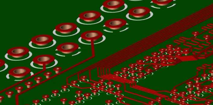
Vias introduce inductance and capacitance, which can affect signal performance. To minimize these effects, designers should use blind and buried vias, which connect only specific layers, reducing the number of layer transitions. Altium Designer supports the use of advanced via structures, allowing designers to optimize the placement and configuration of vias for high-speed signals.
Power integrity is also a key factor in high-speed PCB design.
Fluctuations in power supply can lead to signal degradation and system instability. To ensure stable power delivery, designers should use power planes and decoupling capacitors strategically. Altium Designer’s power distribution network analysis tools help identify potential issues and optimize the placement of decoupling capacitors to maintain a stable power supply.
In conclusion, advanced routing techniques are essential for high-speed PCB design in Altium. By carefully managing impedance, signal return paths, crosstalk, length matching, via structures, and power integrity, designers can achieve optimal performance and signal integrity. Altium Designer provides a comprehensive set of tools to address these challenges, enabling designers to create high-speed PCBs that meet the stringent requirements of modern electronic systems.

