High speed pcb design analysis
Signal Integrity Challenges in High Speed PCB Design
In the realm of high-speed printed circuit board (PCB) design, signal integrity challenges are paramount considerations that can significantly impact the performance and reliability of electronic systems. As the demand for faster data transmission rates and higher processing speeds continues to escalate, engineers are increasingly confronted with the complexities associated with maintaining signal integrity. This article delves into the various signal integrity challenges that arise in high-speed PCB design, elucidating the underlying causes and potential mitigation strategies.
One of the primary challenges in high-speed PCB design is the issue of signal reflection.
When a signal travels along a transmission line, any impedance discontinuity can cause a portion of the signal to be reflected back towards the source. This phenomenon can lead to signal degradation, data corruption, and increased electromagnetic interference (EMI). To address this, designers must ensure that the characteristic impedance of the transmission line is matched to the source and load impedances. Techniques such as controlled impedance routing and the use of termination resistors are commonly employed to minimize reflections and enhance signal integrity.
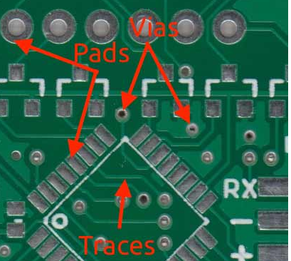
Another significant challenge is crosstalk, which occurs when a signal on one trace induces an unwanted signal on an adjacent trace.
Crosstalk can be particularly problematic in densely packed PCBs where traces are routed in close proximity. The resulting interference can lead to erroneous data transmission and compromised system performance. To mitigate crosstalk, designers can implement strategies such as increasing the spacing between traces, using differential signaling, and incorporating ground planes to provide effective shielding. Additionally, careful layer stack-up design can help to isolate high-speed signals and reduce the potential for crosstalk.
Signal attenuation is also a critical concern in high-speed PCB design.
As signals propagate through the PCB material, they experience losses due to the resistive, capacitive, and inductive properties of the transmission medium. These losses can result in reduced signal amplitude and increased rise and fall times, ultimately affecting the integrity of the transmitted data. To combat signal attenuation, designers can select low-loss PCB materials, optimize trace widths and lengths, and employ signal conditioning techniques such as equalization and pre-emphasis.
Electromagnetic interference (EMI) poses another formidable challenge in high-speed PCB design.
High-speed signals can radiate electromagnetic energy, which can interfere with other electronic components and systems. Conversely, external sources of EMI can disrupt the operation of high-speed circuits. To mitigate EMI, designers can implement shielding techniques, such as using ground planes and metal enclosures, and ensure proper grounding and decoupling practices. Additionally, adhering to design guidelines for trace routing, such as avoiding sharp bends and minimizing loop areas, can help to reduce EMI emissions.
Power integrity is closely related to signal integrity and is a crucial aspect of high-speed PCB design.
Fluctuations in the power supply can introduce noise into the signal paths, leading to data errors and system instability. To ensure power integrity, designers must provide adequate decoupling capacitance, design robust power distribution networks, and minimize power supply noise. Techniques such as using multiple power and ground planes, implementing power islands, and employing low-inductance vias can enhance power integrity and support the reliable operation of high-speed circuits.
In conclusion, signal integrity challenges in high-speed PCB design are multifaceted and require a comprehensive understanding of the underlying principles and potential mitigation strategies. By addressing issues such as signal reflection, crosstalk, signal attenuation, electromagnetic interference, and power integrity, designers can enhance the performance and reliability of high-speed electronic systems. As technology continues to advance, the importance of maintaining signal integrity in high-speed PCB design will only become more pronounced, necessitating ongoing innovation and refinement in design practices.
Techniques for Minimizing Crosstalk in High Speed PCBs
In the realm of high-speed printed circuit board (PCB) design, minimizing crosstalk is a critical concern. Crosstalk, the unwanted coupling of signals between adjacent traces, can lead to signal integrity issues, data corruption, and overall system malfunction. To address this, designers employ a variety of techniques aimed at reducing crosstalk and ensuring reliable performance.
One fundamental approach to minimizing crosstalk is through careful trace routing.
By maintaining adequate spacing between signal traces, designers can significantly reduce the potential for electromagnetic interference. The general rule of thumb is to keep the distance between traces at least three times the width of the trace itself. This spacing helps to mitigate the capacitive and inductive coupling that leads to crosstalk. Additionally, routing high-speed signals on different layers, separated by a ground plane, can further isolate them and reduce interference.
Another effective technique involves the use of differential signaling.
Differential pairs, consisting of two complementary signals, are routed closely together. This configuration allows the electromagnetic fields generated by each signal to cancel each other out, thereby reducing the potential for crosstalk. Moreover, differential pairs are less susceptible to external noise, making them ideal for high-speed data transmission.
Ground planes play a crucial role in minimizing crosstalk.
A continuous ground plane provides a low-impedance return path for signals, which helps to contain electromagnetic fields and reduce coupling between traces. Ensuring that the ground plane is unbroken and free of splits or gaps is essential for maintaining signal integrity. In multilayer PCBs, placing a ground plane adjacent to signal layers can further enhance isolation and reduce crosstalk.
The use of guard traces is another technique employed to combat crosstalk.
Guard traces are grounded traces placed between signal lines to act as a shield. These traces absorb and redirect the electromagnetic fields, preventing them from coupling into adjacent signal lines. While guard traces can be effective, they require careful implementation to avoid creating additional impedance discontinuities.
Impedance control is also vital in high-speed PCB design.
Ensuring that traces have a consistent impedance along their length helps to minimize reflections and signal degradation. Controlled impedance can be achieved through careful selection of trace width, spacing, and the dielectric properties of the PCB material. By maintaining consistent impedance, designers can reduce the likelihood of crosstalk and improve overall signal integrity.
In addition to these techniques, proper termination of signal lines is essential.
Termination resistors, placed at the end of signal traces, help to match the impedance of the trace and the load, thereby reducing reflections and crosstalk. There are various termination methods, including series, parallel, and Thevenin termination, each with its own advantages and considerations.
Finally, signal integrity analysis tools and simulation software are invaluable in the design process.
These tools allow designers to model and predict the behavior of high-speed signals, identify potential sources of crosstalk, and optimize the PCB layout accordingly. By leveraging these advanced tools, designers can make informed decisions and implement effective strategies to minimize crosstalk.
In conclusion, minimizing crosstalk in high-speed PCB design requires a multifaceted approach. Through careful trace routing, differential signaling, the use of ground planes and guard traces, impedance control, proper termination, and the use of simulation tools, designers can effectively reduce crosstalk and ensure reliable performance. By adhering to these techniques, high-speed PCBs can achieve the signal integrity necessary for modern electronic systems.
Importance of Power Integrity in High Speed PCB Design
In the realm of high-speed PCB design, power integrity emerges as a critical factor that can significantly influence the performance and reliability of electronic systems. As electronic devices continue to evolve, demanding higher speeds and greater functionality, ensuring robust power integrity becomes paramount. Power integrity refers to the ability of the power delivery network (PDN) within a PCB to provide a stable and noise-free power supply to all active components. This stability is crucial for maintaining the proper operation of high-speed circuits, which are highly sensitive to variations in power supply.
One of the primary reasons power integrity is so vital in high-speed PCB design is the increasing complexity and density of modern electronic circuits.
As the number of components on a PCB grows, so does the demand for a consistent and reliable power supply. Any fluctuations or noise in the power delivery can lead to signal integrity issues, causing data errors, timing problems, and even complete system failures. Therefore, designers must meticulously plan and analyze the PDN to ensure it can meet the stringent requirements of high-speed applications.
Moreover, the rise in operating frequencies exacerbates the challenges associated with power integrity.
Higher frequencies result in faster switching times, which in turn generate more significant transient currents. These transients can induce voltage drops and noise within the PDN, potentially disrupting the operation of sensitive components. To mitigate these effects, designers often employ techniques such as decoupling capacitors, which help to filter out high-frequency noise and stabilize the power supply. However, the placement and selection of these capacitors require careful consideration to be effective.
In addition to decoupling strategies, the layout of the PCB itself plays a crucial role in maintaining power integrity.
The physical arrangement of power and ground planes, as well as the routing of power traces, can significantly impact the performance of the PDN. For instance, a well-designed power plane can provide a low-impedance path for current flow, reducing the potential for voltage drops and noise. Conversely, poor layout practices, such as long and narrow power traces, can introduce inductance and resistance, degrading power integrity.
Furthermore, the choice of materials and stack-up configuration in a PCB can influence power integrity.
High-speed designs often require low-loss materials to minimize signal attenuation and maintain signal integrity. These materials can also affect the impedance of the power delivery network, necessitating careful selection to ensure compatibility with the overall design requirements. Additionally, the stack-up configuration, which defines the arrangement of layers within the PCB, must be optimized to provide adequate power distribution while minimizing electromagnetic interference (EMI).
Simulation and modeling tools are indispensable in the analysis and optimization of power integrity in high-speed PCB design.
These tools allow designers to predict the behavior of the PDN under various operating conditions, identify potential issues, and evaluate the effectiveness of different design strategies. By leveraging these tools, designers can make informed decisions and implement solutions that enhance power integrity, ultimately leading to more reliable and efficient electronic systems.
In conclusion, power integrity is a fundamental aspect of high-speed PCB design that cannot be overlooked. As electronic devices continue to push the boundaries of performance, ensuring a stable and noise-free power supply becomes increasingly challenging. Through careful planning, strategic component placement, optimized layout practices, and the use of advanced simulation tools, designers can address these challenges and achieve robust power integrity. This, in turn, ensures the reliable operation of high-speed circuits, paving the way for the continued advancement of electronic technology.
Advanced Simulation Tools for High Speed PCB Analysis
In the realm of high-speed PCB design, the importance of advanced simulation tools cannot be overstated. As electronic devices continue to evolve, the demand for faster and more efficient circuit boards has surged, necessitating the use of sophisticated simulation techniques to ensure optimal performance. These tools play a crucial role in predicting and mitigating potential issues that could arise in high-speed circuits, thereby enhancing the reliability and functionality of the final product.
One of the primary benefits of advanced simulation tools is their ability to model complex electromagnetic interactions within a PCB.
High-speed circuits are particularly susceptible to issues such as signal integrity, electromagnetic interference (EMI), and crosstalk. By utilizing simulation software, designers can visualize how signals propagate through the board and identify areas where these problems might occur. This predictive capability allows for the early detection of potential issues, enabling designers to make necessary adjustments before physical prototypes are created.
Moreover, advanced simulation tools facilitate the analysis of power integrity, which is critical in high-speed PCB design.
Power integrity issues can lead to voltage fluctuations and noise, adversely affecting the performance of the circuit. Simulation tools can model the power distribution network (PDN) and help designers optimize the placement of decoupling capacitors and other components to ensure a stable power supply. This level of analysis is essential for maintaining the integrity of high-speed signals and preventing performance degradation.
Transitioning to another significant aspect, thermal management is another area where advanced simulation tools prove invaluable.
High-speed circuits generate substantial amounts of heat, which can impact the reliability and longevity of the PCB. Simulation tools can predict thermal behavior and identify hotspots within the design. By analyzing these thermal profiles, designers can implement effective cooling strategies, such as heat sinks or thermal vias, to dissipate heat efficiently. This proactive approach to thermal management ensures that the PCB operates within safe temperature limits, thereby enhancing its overall reliability.
Furthermore, advanced simulation tools offer the advantage of iterative design optimization.
In traditional design processes, multiple physical prototypes are often required to refine the PCB layout, which can be time-consuming and costly. Simulation tools, on the other hand, allow for virtual prototyping, enabling designers to test various configurations and make iterative improvements without the need for physical iterations. This not only accelerates the design process but also reduces development costs, making it a highly efficient approach to high-speed PCB design.
In addition to these technical benefits, advanced simulation tools also facilitate collaboration among design teams.
Modern simulation software often includes features that allow for seamless sharing of design data and simulation results. This collaborative environment enables different team members, such as electrical engineers, thermal analysts, and signal integrity specialists, to work together more effectively. By fostering better communication and collaboration, these tools help ensure that all aspects of the PCB design are thoroughly analyzed and optimized.
In conclusion, advanced simulation tools are indispensable in the field of high-speed PCB design. They provide a comprehensive platform for analyzing and optimizing various aspects of the design, from signal integrity and power integrity to thermal management and iterative optimization. By leveraging these tools, designers can predict and mitigate potential issues, enhance collaboration, and ultimately deliver high-performance, reliable PCBs that meet the ever-increasing demands of modern electronic devices.