High-Speed PCB Power Decoupling Design Guide
1. Introduction
In high-speed printed circuit board (PCB) designs, maintaining stable power delivery is critical to ensuring signal integrity, reducing electromagnetic interference (EMI), and preventing voltage fluctuations. Power decoupling is a fundamental technique used to mitigate noise and provide instantaneous current to integrated circuits (ICs). This guide provides a comprehensive overview of power decoupling strategies for high-speed PCBs, including capacitor selection, placement, and layout optimization.
2. The Importance of Power Decoupling
2.1 Power Distribution Network (PDN) Challenges
High-speed digital circuits demand rapid current transitions, leading to transient voltage drops (ΔI noise) due to parasitic inductance and resistance in the power delivery path. Without proper decoupling, these fluctuations can cause:
- Signal integrity degradation (ringing, ground bounce)
- Increased EMI emissions
- Timing errors and false switching
2.2 Decoupling Capacitor Functions
Decoupling capacitors serve two primary roles:
- Bulk Energy Storage: Large capacitors (e.g., electrolytic, tantalum) supply sustained current during prolonged demand.
- High-Frequency Noise Suppression: Small ceramic capacitors (e.g., 0.1 µF, 0.01 µF) provide instantaneous charge for fast switching ICs.
3. Decoupling Capacitor Selection
3.1 Capacitor Types and Their Applications
| Capacitor Type | Typical Values | Frequency Range | Use Case |
|---|---|---|---|
| Electrolytic | 10 µF – 1000 µF | Low-frequency (<1 MHz) | Bulk decoupling |
| Tantalum | 1 µF – 100 µF | Mid-frequency (1–10 MHz) | Intermediate storage |
| Ceramic (X7R, X5R) | 0.01 µF – 1 µF | High-frequency (10–100 MHz) | Local IC decoupling |
| MLCC (NPO, C0G) | 1 pF – 10 nF | Ultra-high-frequency (>100 MHz) | RF and high-speed ICs |
3.2 Key Parameters
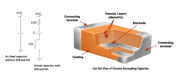
- Equivalent Series Resistance (ESR): Lower ESR reduces voltage ripple.
- Equivalent Series Inductance (ESL): Minimizing ESL improves high-frequency performance.
- Self-Resonant Frequency (SRF): Capacitors are most effective near their SRF.
4. Optimizing Decoupling Capacitor Placement
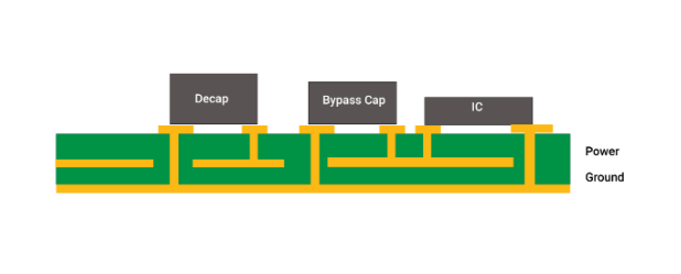
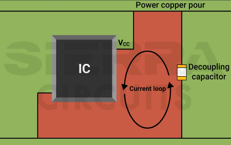
4.1 The “Close to the IC” Rule
- Place decoupling capacitors as close as possible to the IC’s power pins.
- Minimize loop inductance by reducing trace lengths between the capacitor and the IC.
4.2 Multi-Capacitor Strategies
- Parallel Capacitors: Use multiple values (e.g., 10 µF, 0.1 µF, 0.01 µF) to cover a wide frequency range.
- Staggered Placement: Distribute capacitors around high-current devices (e.g., FPGAs, processors).
4.3 Power and Ground Plane Considerations
- Use low-impedance power planes to reduce PDN noise.
- Ensure short via connections to minimize inductance.

5. PCB Layout Best Practices
5.1 Minimizing Loop Inductance
- Use wide traces or power planes for capacitor connections.
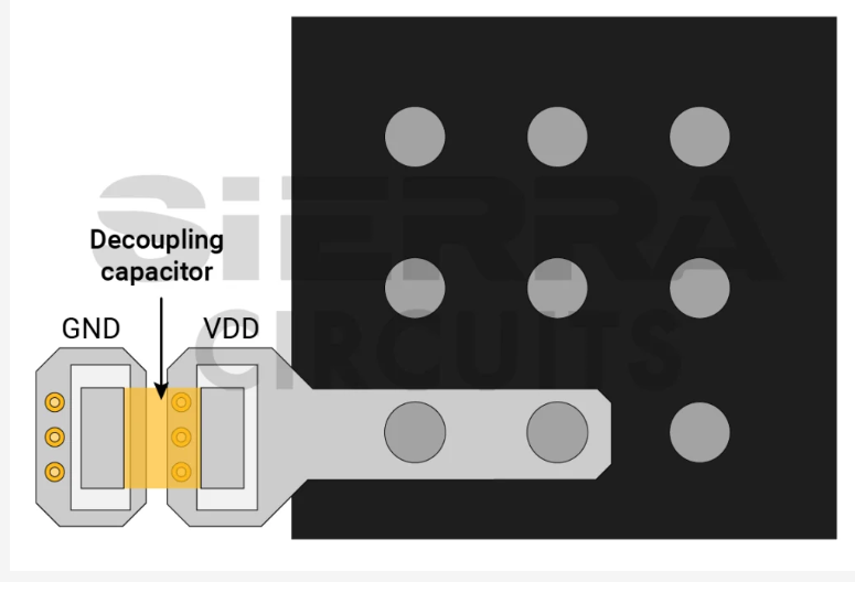
- Place ground vias adjacent to power vias to reduce loop area.
5.2 Via Placement and Routing
- Multiple vias reduce parasitic inductance.
- Avoid daisy-chaining capacitors—connect each directly to the power plane.
5.3 Layer Stackup Optimization
- Dedicate adjacent power and ground planes for low-impedance return paths.
- Use thin dielectric layers between power and ground to enhance capacitance.
6. Simulation and Measurement Techniques
6.1 PDN Impedance Analysis
- Simulate PDN impedance using tools like ANSYS SIwave, Cadence Sigrity, or Keysight ADS.
- Target impedance (Ztarget) is calculated as:
[
Z_{target} = \frac{\Delta V}{\Delta I}
]
where ΔV is the allowable voltage ripple and ΔI is the current transient.
6.2 Time-Domain and Frequency-Domain Testing
- Oscilloscope measurements detect voltage droops and noise.
- Vector Network Analyzer (VNA) tests PDN impedance up to GHz frequencies.
7. Advanced Decoupling Techniques
7.1 Embedded Capacitance
- Thin-core dielectrics (e.g., 2–4 µm) provide distributed capacitance.
- Reduces the need for discrete capacitors in ultra-high-speed designs.
7.2 Active Decoupling
- Uses active voltage regulators (LDOs, switching regulators) near ICs for dynamic response.
7.3 Package-Level Decoupling
- On-package capacitors (e.g., Intel’s FIVR) minimize inductance for CPUs and GPUs.
8. Common Mistakes to Avoid
- Insufficient capacitor variety (only using 0.1 µF capacitors).
- Long decoupling capacitor traces increasing inductance.
- Ignoring return current paths, leading to ground loops.
- Overlooking high-frequency capacitor requirements in RF/mixed-signal designs.
9. Conclusion
Effective power decoupling is essential for high-speed PCB performance. By selecting appropriate capacitors, optimizing placement, and following best layout practices, designers can minimize noise, improve signal integrity, and ensure reliable operation. Simulation and measurement validation further enhance PDN robustness, making decoupling a critical step in modern PCB design.