High-speed pcb primer for sata pcie usb 2.0 and hdmi
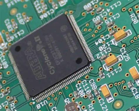
High speed PCB refers to a printed circuit board (PCB) that is designed to handle high-frequency signals with minimal signal loss or distortion.
These types of PCBs are typically used in electronic devices that require fast data transfer rates,
such as computers, smartphones, and other digital devices.
High speed PCBs are designed with specialized materials and techniques that minimize signal reflections, crosstalk, and electromagnetic interference (EMI).
They also feature controlled impedance, which ensures that the electrical properties of the PCB are consistent across all traces and components.

1. SATA:
Serial ATA (SATA) is a high-speed interface used for connecting storage devices such as hard drives and solid-state drives.
To design a high-speed PCB for SATA, it is important to consider the signal integrity and impedance matching of the traces.
The differential pairs should be routed as close as possible and with minimal length differences to ensure proper signal transmission.
2. PCIe:
Peripheral Component Interconnect Express (PCIe) is a high-speed serial interface used for connecting devices such as graphics cards and network adapters. To design a high-speed PCB for PCIe,
it is important to consider the routing of differential pairs and the use of impedance-controlled traces.
The traces should be routed with minimal length differences and with proper termination to ensure proper signal transmission.
3. USB 2.0:
Universal Serial Bus (USB) 2.0 is a high-speed interface used for connecting devices such as printers, cameras, and external hard drives.
To design a high-speed PCB for USB 2.0, it is important to consider the signal integrity of the traces.
The traces should be routed with proper impedance matching and with minimal length differences to ensure proper signal transmission.
4. HDMI:
High-Definition Multimedia Interface (HDMI) is a high-speed interface used for connecting devices such as TVs and monitors.
To design a high-speed PCB for HDMI, it is important to consider the signal integrity of the traces.
The traces should be routed with proper impedance matching and with minimal length differences to ensure proper signal transmission.
In addition to the above considerations, it is important to follow best practices for high-speed PCB design,
such as minimizing the use of vias, keeping the traces short and straight, and using proper grounding techniques.
By following these guidelines, you can ensure that your high-speed PCB design for SATA, PCIe,
USB 2.0, and HDMI interfaces will meet the necessary performance requirements.

high speed pcb layout techniques texas instruments
Texas Instruments (TI) offers several high-speed PCB layout techniques to help designers optimize their PCB designs for high-speed applications. Some of these techniques include:
1. Differential Pair Routing:
Differential pairs are used to transmit high-speed signals with minimal noise and interference.
TI recommends routing differential pairs as close together as possible to reduce crosstalk and using a ground plane between the pairs to minimize EMI.
2. Via Placement:
Placing vias too close to high-speed signals can cause signal reflections and distortions.
TI recommends placing vias at least three times the trace width away from the signal trace and using blind vias or buried vias to reduce signal reflections.
3. Signal Return Paths:
High-speed signals require a low-impedance return path to minimize signal reflections.
TI recommends using a ground plane or power plane as a return path and placing decoupling capacitors near the signal source to reduce noise.
4. Controlled Impedance:
High-speed signals require a consistent impedance to prevent signal reflections.
TI recommends using controlled impedance traces and vias to ensure the electrical properties of the PCB are consistent across all traces and components.
5. Power Integrity:
High-speed signals require a stable power supply to prevent noise and interference.
TI recommends using multiple power planes, decoupling capacitors, and minimizing the loop area of the power supply to improve power integrity.
By following these high-speed PCB layout techniques recommended by Texas Instruments,
designers can optimize their PCB designs for high-speed applications and minimize signal loss, noise, and interference.