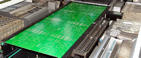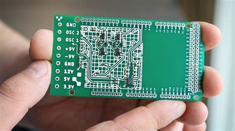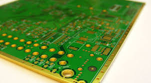
High speed pcb signal
Understanding Signal Integrity in High Speed PCB signal Design
In the realm of high-speed printed circuit board (PCB) design, understanding signal integrity is paramount to ensuring optimal performance and reliability of electronic systems. As technology advances, the demand for faster data transmission rates has led to the development of high-speed PCBs, which are integral to modern electronic devices. However, with increased speed comes the challenge of maintaining signal integrity, a critical aspect that can significantly impact the functionality of a device.
Signal integrity refers to the quality and reliability of electrical signals as they travel through a PCB.
In high-speed designs, signals are susceptible to various forms of degradation, including reflections, crosstalk, and electromagnetic interference (EMI). These issues can distort the signal, leading to data errors and system malfunctions. Therefore, understanding and mitigating these factors is essential for engineers working on high-speed PCB designs.
One of the primary concerns in high-speed PCB design is reflections, which occur when a signal encounters an impedance mismatch along its transmission path.
This mismatch can cause a portion of the signal to be reflected back towards the source, resulting in signal distortion. To minimize reflections, it is crucial to ensure impedance matching throughout the PCB. This can be achieved by carefully designing the trace geometry and selecting appropriate materials that maintain consistent impedance levels.
In addition to reflections, crosstalk is another significant issue that affects signal integrity.
Crosstalk occurs when a signal in one trace induces an unwanted signal in an adjacent trace, leading to interference and potential data corruption. To mitigate crosstalk, designers can employ techniques such as increasing the spacing between traces, using differential signaling, and implementing ground planes to provide effective isolation between signal paths.
Moreover, electromagnetic interference poses a substantial threat to signal integrity in high-speed PCBs.
EMI can originate from both internal and external sources, disrupting the normal operation of electronic components. To combat EMI, designers can utilize shielding techniques, such as enclosing sensitive components in metal enclosures or using ground planes to absorb and redirect electromagnetic fields. Additionally, careful layout planning and the strategic placement of components can help minimize EMI exposure.
Transitioning from understanding these challenges to implementing solutions, it is essential for engineers to employ advanced simulation tools during the design phase.
These tools allow for the modeling and analysis of signal behavior, enabling designers to identify potential issues and optimize the PCB layout before physical prototyping. By simulating various scenarios, engineers can make informed decisions regarding trace routing, layer stack-up, and component placement, ultimately enhancing signal integrity.
Furthermore, collaboration between design and manufacturing teams is crucial to ensure that the theoretical design translates effectively into a functional PCB.
Manufacturing processes can introduce variations that affect signal integrity, such as etching inaccuracies or material inconsistencies. By maintaining open communication and adhering to design-for-manufacturability principles, potential discrepancies can be addressed early in the process, reducing the risk of signal integrity issues in the final product.
In conclusion, understanding signal integrity in high-speed PCB design is a multifaceted challenge that requires a comprehensive approach. By addressing factors such as reflections, crosstalk, and EMI, and leveraging advanced simulation tools, engineers can enhance the performance and reliability of high-speed electronic systems. As technology continues to evolve, the importance of maintaining signal integrity will only grow, underscoring the need for ongoing research and innovation in this critical field.
Techniques for Minimizing Crosstalk in High-Speed PCBs
In the realm of high-speed printed circuit boards (PCBs), managing signal integrity is paramount to ensuring optimal performance. One of the most critical challenges faced by engineers is minimizing crosstalk, which refers to the unwanted coupling of signals between adjacent traces. As data rates increase, the susceptibility to crosstalk becomes more pronounced, necessitating the implementation of effective techniques to mitigate its impact.
To begin with, understanding the root causes of crosstalk is essential.
Crosstalk primarily arises due to electromagnetic interference between signal traces that are in close proximity. This interference can lead to signal degradation, increased error rates, and ultimately, compromised system performance. Therefore, the first step in minimizing crosstalk is to carefully consider the physical layout of the PCB. By increasing the spacing between traces, engineers can significantly reduce the potential for electromagnetic coupling. This simple yet effective strategy is often the first line of defense against crosstalk.
In addition to spacing, the use of ground planes is another crucial technique.
Ground planes act as a shield, absorbing and redirecting electromagnetic interference away from sensitive signal traces. By strategically placing ground planes adjacent to signal layers, engineers can create a controlled environment that minimizes crosstalk. Moreover, employing a multi-layer PCB design allows for the separation of signal and ground layers, further enhancing the board’s ability to mitigate interference.
Transitioning from layout considerations, the choice of materials also plays a vital role in crosstalk reduction.
High-speed PCBs benefit from materials with low dielectric constants and low loss tangents, as these properties help maintain signal integrity over long distances. Additionally, selecting materials with high thermal stability ensures that the PCB can withstand the heat generated by high-speed operations without compromising performance.
Furthermore, differential signaling is a technique that can effectively combat crosstalk.
By transmitting signals as differential pairs, engineers can take advantage of the inherent noise-canceling properties of this configuration. Differential pairs are less susceptible to external interference, as any noise that does couple into the signals tends to affect both lines equally, allowing it to be canceled out at the receiver. This method not only reduces crosstalk but also enhances the overall robustness of the signal transmission.
Another technique involves the use of termination resistors.
Properly terminating signal traces with resistors can prevent signal reflections, which are a common source of crosstalk. By matching the impedance of the trace to the termination resistor, engineers can ensure that signals are absorbed rather than reflected back along the trace, thereby minimizing interference with adjacent signals.
Finally, simulation and modeling tools are indispensable in the design process.
These tools allow engineers to predict and analyze potential crosstalk issues before the physical PCB is manufactured. By simulating different scenarios and configurations, engineers can identify and address potential problems early in the design phase, saving time and resources in the long run.
In conclusion, minimizing crosstalk in high-speed PCBs requires a multifaceted approach that encompasses careful layout design, material selection, and the implementation of specific techniques such as differential signaling and termination. By understanding and addressing the factors that contribute to crosstalk, engineers can ensure that high-speed PCBs operate with the highest level of signal integrity, ultimately leading to more reliable and efficient electronic systems.
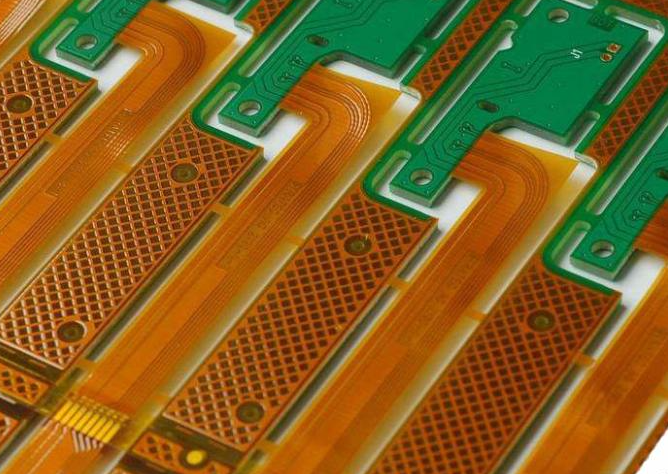
The Role of Dielectric Materials in High-Speed PCB Performance
In the realm of high-speed printed circuit boards (PCBs), the choice of dielectric materials plays a pivotal role in determining the overall performance and reliability of the system. As electronic devices continue to evolve, demanding faster data transmission rates and higher frequencies, the importance of selecting appropriate dielectric materials becomes increasingly critical.
These materials, which serve as insulators between conductive layers, significantly influence signal integrity, impedance control, and thermal management, all of which are essential for the optimal functioning of high-speed PCBs.
To begin with, dielectric materials impact the signal integrity of high-speed PCBs by affecting the propagation of electromagnetic waves through the board.
The dielectric constant, or relative permittivity, of a material determines how much it can store electrical energy. A lower dielectric constant is generally preferred for high-speed applications as it allows signals to travel faster and with less distortion. This is because a lower dielectric constant reduces the capacitive loading on the signal traces, thereby minimizing signal delay and attenuation. Consequently, selecting a dielectric material with an appropriate dielectric constant is crucial for maintaining signal integrity and ensuring that high-speed signals are transmitted accurately and efficiently.
Moreover, dielectric materials play a significant role in impedance control, which is vital for minimizing signal reflections and losses.
Impedance mismatches can lead to signal reflections, causing data errors and degrading the performance of high-speed PCBs. The characteristic impedance of a transmission line is influenced by the dielectric material’s properties, including its dielectric constant and thickness. By carefully selecting and controlling these parameters, designers can achieve the desired impedance levels, thereby reducing signal reflections and enhancing the overall performance of the PCB. This highlights the importance of dielectric materials in achieving precise impedance control, which is essential for high-speed applications.
In addition to signal integrity and impedance control, dielectric materials also contribute to the thermal management of high-speed PCBs.
As electronic devices operate at higher speeds and frequencies, they generate more heat, which can adversely affect the performance and reliability of the system. Dielectric materials with high thermal conductivity can help dissipate heat more effectively, preventing overheating and ensuring the longevity of the PCB. Furthermore, materials with low thermal expansion coefficients are preferred, as they minimize mechanical stress and potential damage caused by temperature fluctuations. Thus, the thermal properties of dielectric materials are crucial for maintaining the stability and reliability of high-speed PCBs.
Furthermore, the choice of dielectric materials can also impact the manufacturability and cost-effectiveness of high-speed PCBs.
Advanced dielectric materials with superior electrical and thermal properties may come at a higher cost, but they can offer significant performance benefits. Therefore, designers must carefully balance performance requirements with budget constraints when selecting dielectric materials. Additionally, the compatibility of these materials with existing manufacturing processes is essential to ensure efficient production and minimize potential issues during fabrication.
In conclusion, the role of dielectric materials in high-speed PCB performance is multifaceted, influencing signal integrity, impedance control, thermal management, and manufacturability. As the demand for faster and more reliable electronic devices continues to grow, the careful selection and optimization of dielectric materials will remain a critical aspect of high-speed PCB design. By understanding and leveraging the properties of these materials, designers can enhance the performance and reliability of high-speed PCBs, meeting the ever-increasing demands of modern electronic applications.
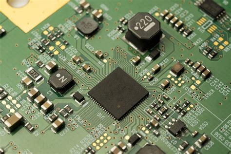
Best Practices for Routing High-Speed Signals on PCBs
Routing high-speed signals on printed circuit boards (PCBs) is a critical task that demands meticulous attention to detail and a comprehensive understanding of electromagnetic principles. As electronic devices become increasingly sophisticated, the need for efficient and reliable high-speed signal transmission has never been more crucial. To achieve optimal performance, engineers must adhere to best practices that mitigate signal integrity issues and ensure seamless communication across the board.
One of the fundamental principles in routing high-speed signals is maintaining controlled impedance.
This involves designing traces with consistent width and spacing to match the characteristic impedance of the transmission line. By doing so, reflections are minimized, and signal integrity is preserved. It is essential to use impedance calculators or simulation tools during the design phase to ensure that the trace dimensions align with the desired impedance values. Furthermore, selecting the appropriate dielectric material for the PCB substrate can significantly impact impedance control, as different materials exhibit varying dielectric constants.
In addition to impedance control, minimizing crosstalk is paramount when routing high-speed signals.
Crosstalk occurs when a signal in one trace induces an unwanted signal in an adjacent trace, potentially leading to data corruption. To mitigate this, designers should maintain adequate spacing between traces and employ differential signaling where possible. Differential pairs, which consist of two complementary signals, are less susceptible to external noise and crosstalk, making them ideal for high-speed applications. Moreover, routing differential pairs with equal lengths ensures that the signals arrive simultaneously at the receiver, further enhancing signal integrity.
Another critical aspect of high-speed PCB design is the management of signal return paths.
High-speed signals tend to follow the path of least inductance, which is typically directly beneath the signal trace on the reference plane. Ensuring a continuous and uninterrupted return path is vital to prevent signal distortion and electromagnetic interference (EMI). Designers should avoid routing high-speed signals over gaps in the reference plane, as this can create impedance discontinuities and increase EMI susceptibility. Instead, maintaining a solid ground plane beneath high-speed traces is recommended to provide a stable return path.
Furthermore, the use of vias in high-speed signal routing should be approached with caution.
Vias introduce parasitic inductance and capacitance, which can degrade signal quality. To minimize these effects, it is advisable to use as few vias as possible and to opt for blind or buried vias when necessary. Additionally, ensuring that vias are properly back-drilled can help reduce their impact on signal integrity by removing unnecessary stubs.
Signal integrity can also be enhanced by employing proper termination techniques.
Termination resistors, when placed correctly, can match the impedance of the transmission line and prevent reflections. Series and parallel termination are common methods used to achieve this, and the choice between them depends on the specific requirements of the design.
In conclusion, routing high-speed signals on PCBs requires a strategic approach that encompasses controlled impedance, crosstalk minimization, effective return path management, judicious use of vias, and appropriate termination techniques. By adhering to these best practices, engineers can ensure that their designs meet the demands of modern high-speed applications, delivering reliable and efficient performance. As technology continues to evolve, staying informed about the latest advancements in PCB design will be essential for maintaining signal integrity and achieving success in high-speed electronic systems.