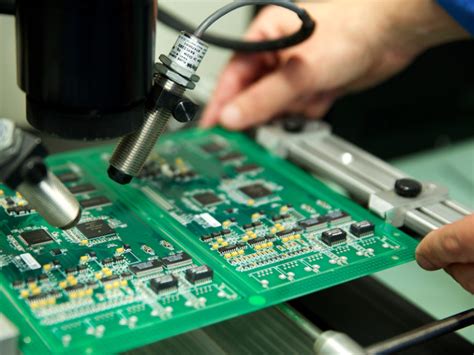
High speed pcb simulation
Importance Of Signal Integrity In High Speed PCB Simulation
In the realm of high-speed printed circuit board (PCB) design, the importance of signal integrity cannot be overstated. As electronic devices become increasingly sophisticated, the demand for faster data transmission rates has surged, necessitating the need for high-speed PCBs. However, with these advancements come significant challenges, particularly in maintaining signal integrity. Signal integrity refers to the quality and reliability of electrical signals as they travel through the PCB. Ensuring signal integrity is crucial because any degradation can lead to data errors, system malfunctions, and overall reduced performance.
One of the primary factors affecting signal integrity in high-speed PCB design is the phenomenon of signal reflection.
When a signal encounters a discontinuity in the transmission path, such as a change in impedance, part of the signal is reflected back towards the source. This reflection can interfere with the original signal, causing distortions and potential data loss. To mitigate this, designers must carefully manage impedance throughout the PCB layout, ensuring that traces are designed with consistent impedance and that any transitions are smooth and well-matched.
Another critical aspect of signal integrity is crosstalk, which occurs when a signal in one trace induces an unwanted signal in an adjacent trace.
This can be particularly problematic in high-speed designs where traces are often placed in close proximity to one another. Crosstalk can lead to noise and interference, degrading the quality of the signal. To address this, designers can employ techniques such as increasing the spacing between traces, using differential signaling, and incorporating ground planes to shield sensitive signals.
Moreover, the issue of electromagnetic interference (EMI) is a significant concern in high-speed PCB design.
High-speed signals can radiate electromagnetic energy, which can interfere with other components and systems. Effective EMI management involves careful PCB layout practices, such as minimizing loop areas, using proper grounding techniques, and incorporating shielding where necessary. Additionally, designers can use simulation tools to predict and mitigate potential EMI issues before physical prototypes are built.
Power integrity is another vital consideration in high-speed PCB simulation.
As data rates increase, so does the demand for stable and clean power delivery. Any fluctuations or noise in the power supply can adversely affect signal integrity. To ensure power integrity, designers must focus on proper decoupling and filtering techniques, as well as optimizing the power distribution network (PDN) to minimize voltage drops and noise.
High-speed PCB simulation tools play an indispensable role in addressing these challenges.
These tools allow designers to model and analyze the behavior of signals within the PCB, identifying potential issues and optimizing the design before fabrication. By simulating signal integrity, crosstalk, EMI, and power integrity, designers can make informed decisions and implement corrective measures early in the design process. This not only saves time and cost but also enhances the overall reliability and performance of the final product.
In conclusion, the importance of signal integrity in high-speed PCB simulation cannot be ignored. As electronic devices continue to evolve, maintaining the quality and reliability of signals is paramount to ensuring optimal performance. By understanding and addressing the various factors that affect signal integrity, such as signal reflection, crosstalk, EMI, and power integrity, designers can create robust and efficient high-speed PCBs. Leveraging advanced simulation tools further empowers designers to predict and mitigate potential issues, ultimately leading to more reliable and high-performing electronic systems.
Techniques For Reducing Crosstalk In High Speed PCB Designs
In the realm of high-speed printed circuit board (PCB) design, crosstalk presents a significant challenge that can compromise the integrity and performance of electronic systems. Crosstalk occurs when a signal transmitted on one circuit or channel creates an undesired effect on another circuit or channel. This phenomenon becomes particularly problematic in high-speed designs where signal frequencies are elevated, and the potential for interference is magnified. To mitigate crosstalk and ensure optimal functionality, several techniques can be employed.
One effective method for reducing crosstalk is the strategic placement of traces.
By increasing the spacing between adjacent signal traces, designers can minimize the capacitive and inductive coupling that leads to crosstalk. This approach is particularly beneficial in high-speed designs where the proximity of traces can significantly influence signal integrity. Additionally, routing high-speed signals on different layers, separated by a ground plane, can further reduce the potential for interference. The ground plane acts as a shield, absorbing and dissipating unwanted electromagnetic energy.
Another crucial technique involves the use of differential signaling.
Differential pairs consist of two complementary signals that are routed together, with one signal being the inverse of the other. This configuration helps to cancel out noise and crosstalk, as any interference that affects one signal will similarly affect the other, thereby maintaining the integrity of the differential signal. Properly matched differential pairs, with consistent spacing and length, are essential for maximizing the benefits of this technique.
Implementing proper termination is also vital in high-speed PCB designs.
Unmatched impedance between the transmission line and the load can result in signal reflections, which contribute to crosstalk. By using termination resistors that match the characteristic impedance of the transmission line, designers can minimize reflections and enhance signal integrity. Both series and parallel termination methods can be employed, depending on the specific requirements of the design.
Grounding and power distribution play a significant role in mitigating crosstalk.
A well-designed ground plane provides a low-impedance return path for signals, reducing the potential for noise and interference. Ensuring that the ground plane is continuous and free of gaps is essential for maintaining signal integrity. Additionally, decoupling capacitors should be strategically placed near power pins to filter out high-frequency noise and stabilize the power supply, further reducing the risk of crosstalk.
Shielding is another effective technique for combating crosstalk in high-speed PCB designs.
By enclosing sensitive signal traces in a conductive shield, designers can prevent external electromagnetic interference from affecting the signals. This approach is particularly useful in environments with high levels of electromagnetic noise. The shield should be connected to the ground plane to ensure proper dissipation of unwanted energy.
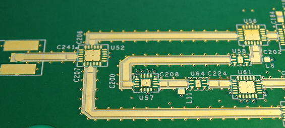
Finally, careful consideration of the PCB layout and stack-up is crucial for minimizing crosstalk.
A well-thought-out stack-up, with alternating signal and ground layers, can significantly reduce the potential for interference. High-speed signals should be routed on internal layers, sandwiched between ground planes, to provide additional shielding and isolation. Additionally, maintaining consistent trace widths and avoiding sharp bends can help preserve signal integrity and reduce the risk of crosstalk.
In conclusion, reducing crosstalk in high-speed PCB designs requires a multifaceted approach that encompasses trace placement, differential signaling, proper termination, grounding, shielding, and thoughtful PCB layout. By employing these techniques, designers can enhance signal integrity, minimize interference, and ensure the reliable performance of high-speed electronic systems.
Role Of Electromagnetic Interference In High Speed PCB Simulation
In the realm of high-speed printed circuit board (PCB) design, the role of electromagnetic interference (EMI) cannot be overstated. As electronic devices become increasingly sophisticated and operate at higher frequencies, the susceptibility to EMI grows, necessitating meticulous simulation and analysis. High-speed PCB simulation serves as a critical tool in predicting and mitigating the adverse effects of EMI, ensuring the reliability and performance of electronic systems.
Electromagnetic interference arises from various sources, both internal and external to the PCB.
Internally, high-speed signals traversing the board can generate electromagnetic fields that interfere with other components and traces. Externally, environmental factors such as nearby electronic devices and power lines can introduce unwanted noise. The complexity of these interactions underscores the importance of comprehensive simulation in the design phase.
One of the primary objectives of high-speed PCB simulation is to identify potential EMI issues before physical prototypes are built.
By employing advanced simulation software, designers can model the electromagnetic behavior of the PCB, taking into account factors such as trace layout, component placement, and grounding schemes. This predictive capability allows for the optimization of the design to minimize EMI, thereby reducing the risk of costly revisions and delays in the development process.
Moreover, high-speed PCB simulation facilitates the analysis of signal integrity, which is closely related to EMI.
Signal integrity refers to the preservation of the quality of electrical signals as they propagate through the PCB. Poor signal integrity can lead to data corruption, timing errors, and overall system instability. Through simulation, designers can evaluate the impact of EMI on signal integrity and implement strategies to enhance signal fidelity, such as impedance matching, differential signaling, and the use of shielding techniques.
Transitioning from the theoretical to the practical, high-speed PCB simulation also aids in compliance with regulatory standards.
Many industries, including telecommunications, automotive, and aerospace, are subject to stringent EMI regulations to ensure the safe and reliable operation of electronic systems. Simulation enables designers to verify that their PCB designs meet these standards, thereby avoiding potential legal and financial repercussions.
Furthermore, the iterative nature of simulation allows for continuous refinement of the PCB design.
As new components are introduced or design requirements evolve, simulation provides a flexible platform for assessing the impact of these changes on EMI performance. This iterative approach not only enhances the robustness of the final product but also accelerates the development timeline by identifying and addressing issues early in the design cycle.
In addition to its technical benefits, high-speed PCB simulation fosters collaboration among multidisciplinary teams.
By providing a common framework for analyzing EMI, simulation tools enable electrical engineers, mechanical engineers, and other stakeholders to work together more effectively. This collaborative environment promotes a holistic understanding of the design challenges and encourages the development of innovative solutions.
In conclusion, the role of electromagnetic interference in high-speed PCB simulation is multifaceted and indispensable. Through the use of advanced simulation techniques, designers can predict and mitigate EMI issues, ensuring signal integrity, regulatory compliance, and overall system reliability. As electronic devices continue to evolve, the importance of high-speed PCB simulation in managing EMI will only grow, underscoring its critical role in the design and development of cutting-edge technologies.
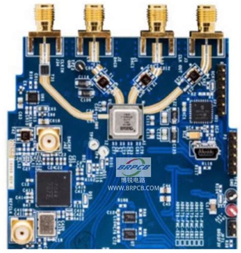
Advanced Tools For High Speed PCB Simulation And Analysis
High-speed PCB simulation and analysis have become indispensable in the design and development of modern electronic systems. As the demand for faster and more efficient electronic devices continues to grow, engineers are increasingly turning to advanced tools to ensure the reliability and performance of their printed circuit boards (PCBs). These tools are essential for identifying potential issues early in the design process, thereby reducing the risk of costly revisions and delays.
One of the primary challenges in high-speed PCB design is managing signal integrity.
As signal frequencies increase, the likelihood of encountering issues such as crosstalk, reflection, and electromagnetic interference (EMI) also rises. Advanced simulation tools enable engineers to model and analyze these phenomena with a high degree of accuracy. By simulating the behavior of signals on the PCB, designers can identify problematic areas and make necessary adjustments before physical prototypes are built. This proactive approach not only saves time but also enhances the overall quality of the final product.
Moreover, power integrity is another critical aspect that must be addressed in high-speed PCB design.
Fluctuations in power delivery can lead to noise and instability, which can severely impact the performance of the electronic system. Advanced simulation tools provide the capability to analyze power distribution networks (PDNs) and identify potential issues such as voltage drops and ground bounce. By optimizing the PDN layout and incorporating appropriate decoupling strategies, engineers can ensure a stable power supply to all components on the PCB.
Thermal management is also a significant concern in high-speed PCB design.
As components operate at higher speeds, they tend to generate more heat, which can affect their performance and longevity. Advanced simulation tools allow engineers to perform thermal analysis, predicting temperature distribution across the PCB and identifying hotspots. This information is crucial for designing effective cooling solutions, such as heat sinks and thermal vias, to dissipate heat efficiently and maintain optimal operating temperatures.
In addition to signal integrity, power integrity, and thermal management, advanced simulation tools also facilitate electromagnetic compatibility (EMC) analysis.
Ensuring that a PCB complies with EMC regulations is essential to prevent interference with other electronic devices and to avoid regulatory issues. Simulation tools can model the electromagnetic emissions from a PCB and help designers implement shielding and filtering techniques to minimize these emissions. This capability is particularly important in applications where stringent EMC standards must be met, such as in automotive and aerospace industries.
Furthermore, the integration of advanced simulation tools with other design software enhances the overall design workflow.
Many simulation tools are now equipped with features that allow seamless integration with PCB layout and schematic capture software. This integration enables a more iterative design process, where simulation results can be quickly incorporated into the design, and changes can be re-simulated to verify their effectiveness. This iterative approach ensures that the final design is robust and meets all performance criteria.
In conclusion, advanced tools for high-speed PCB simulation and analysis are crucial for addressing the complex challenges associated with modern electronic design. By providing accurate modeling and analysis capabilities, these tools enable engineers to optimize signal integrity, power integrity, thermal management, and electromagnetic compatibility. The integration of these tools with other design software further streamlines the design process, ensuring that high-speed PCBs are reliable, efficient, and compliant with industry standards. As technology continues to evolve, the importance of advanced simulation tools in high-speed PCB design will only continue to grow.