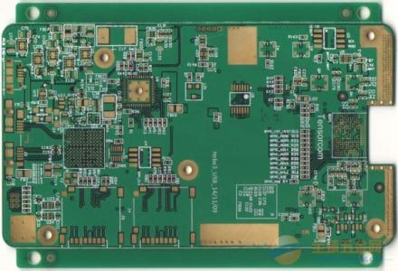
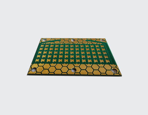
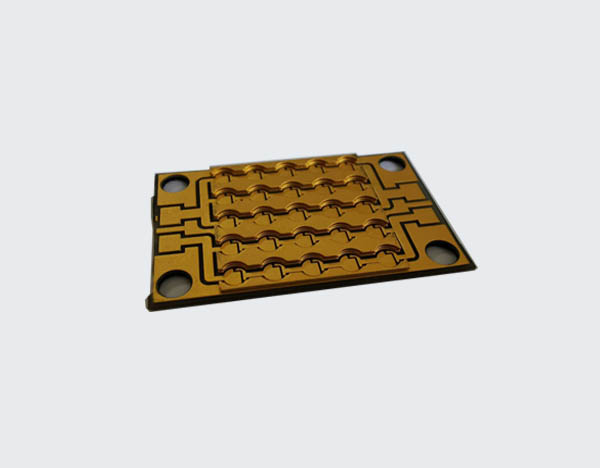
High speed rf pcb design
High-speed RF PCB design refers to the process of designing printed circuit boards that are optimized for high-frequency signals,
typically in the range of 1 GHz to 100 GHz.
These types of PCBs are commonly used in applications such as wireless communications, radar systems, and satellite communications.

The key considerations in high-speed RF PCB design include:
1. Impedance control:
High-frequency signals are very sensitive to changes in impedance, so it is important to carefully control the impedance of the PCB traces, vias, and connectors.
2. Signal integrity:
High-speed signals are prone to reflection, crosstalk, and other types of interference, so it is important to design the PCB layout to minimize these effects.
3. Grounding:
A good grounding scheme is critical for high-speed RF PCBs, as it helps to reduce noise and improve signal quality.
4. Component placement:
The placement of components on the PCB can have a significant impact on signal quality,
so it is important to carefully consider the placement of components such as amplifiers, filters, and antennas.
5. Material selection:
The choice of PCB material can have a significant impact on signal quality,
so it is important to select a material with the appropriate dielectric constant and loss tangent for the desired frequency range.
Overall, high-speed RF PCB design requires careful attention to detail and a thorough understanding of the principles of high-frequency circuit design.
high speed rf pcb design source
There are many sources for high speed RF PCB design, including:
1. Altium Designer:
This is a popular PCB design software that has a range of features specifically for high speed RF design.
2. Keysight ADS:
This is a software suite that includes tools for RF and microwave design, including PCB layout.
3. Cadence Allegro:
This is another popular PCB design software that has features for high speed RF design.
4. Ansys HFSS:
This is a simulation software that can be used to optimize the performance of high speed RF designs.
5. Signal Integrity Journal:
This is an online resource that provides articles, webinars, and other information on high speed PCB design.
6. IEEE Transactions on Microwave Theory and Techniques:
This is a peer-reviewed journal that publishes research on high speed RF design.
7. Texas Instruments:
This company provides a range of resources for high speed RF design, including application notes, white papers, and online training.
8. Analog Devices:
This company also provides resources for high speed RF design, including application notes and online training.
9. RF Design Magazine:
This is a print and online publication that provides articles and news on RF and microwave design.
10. Microwave Journal:
This is another print and online publication that covers RF and microwave design, including high speed PCB design.
1. Layer Stackup:
The layer stackup is a critical aspect of high-speed PCB design.
The number of layers, the thickness of each layer, and the placement of signal and power planes all play a role in determining the performance of the PCB.
2. Signal Integrity:
High-speed signals are susceptible to noise and interference,
which can lead to signal degradation and ultimately affect the performance of the system.
Proper signal integrity analysis and design techniques such as impedance matching, termination, and routing are essential to ensure reliable signal transmission.
3. Power Integrity:
High-speed PCBs require a stable power supply to ensure proper functioning.
Power integrity analysis and design techniques such as decoupling capacitors, power planes,
and voltage regulation must be considered to ensure stable power delivery.
4. Component Placement:
Component placement is critical in high-speed PCB design.
The placement of components affects signal paths, signal integrity, and thermal management.
Proper placement of components, especially high-speed components such as microprocessors and memory,
can significantly improve the performance of the PCB.
5. Routing:
Proper routing of high-speed signals is essential to ensure signal integrity.
Techniques such as differential signaling, length matching, and avoiding vias in signal paths can help reduce signal degradation.
6. Thermal Management:
High-speed PCBs generate a significant amount of heat, which can affect the performance and reliability of the system.
Proper thermal management techniques such as heat sinks, thermal vias, and airflow must be considered to ensure proper heat dissipation.
In conclusion, high-speed multilayer PCB design requires careful consideration of various factors to ensure reliable and high-performance operation.
Proper design techniques and analysis tools can help ensure that the PCB meets the required specifications.