High speed serial and parallel buses on pcb schematics
Understanding High-Speed Serial Bus Design in PCB Schematics
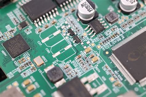
In the realm of printed circuit board (PCB) design, the integration of high-speed serial and parallel buses is a critical consideration for ensuring optimal performance and functionality.
As electronic devices continue to evolve, the demand for faster data transmission rates has led to the widespread adoption of high-speed buses in PCB schematics.
Understanding the intricacies of high-speed serial bus design is essential for engineers and designers aiming to create efficient and reliable electronic systems.
High-speed serial buses, such as PCIe, USB, and SATA, have become the backbone of modern electronic communication. These buses offer several advantages over traditional parallel buses, including reduced pin count, lower electromagnetic interference (EMI), and the ability to achieve higher data rates.
The transition from parallel to serial communication has been driven by the need for increased bandwidth and the miniaturization of electronic components.
Consequently, designers must pay careful attention to the layout and routing of these buses on PCB schematics to mitigate potential issues such as signal integrity and crosstalk.
Signal integrity is a paramount concern in high-speed serial bus design.
As data rates increase, the potential for signal degradation becomes more pronounced. Factors such as impedance mismatches, reflections, and attenuation can significantly impact the quality of the transmitted signal. To address these challenges, designers employ various techniques, including controlled impedance routing, differential signaling, and the use of termination resistors. Controlled impedance routing ensures that the characteristic impedance of the transmission line matches the impedance of the bus, minimizing reflections and signal loss. Differential signaling, on the other hand, involves transmitting data over two complementary signals, which helps to cancel out common-mode noise and improve signal integrity.
In addition to signal integrity, crosstalk is another critical issue that designers must contend with when working with high-speed serial buses.
Crosstalk occurs when a signal on one trace induces an unwanted signal on an adjacent trace, potentially leading to data corruption. To mitigate crosstalk, designers can increase the spacing between traces, use ground planes to provide shielding, and employ differential pairs to reduce susceptibility to interference. These strategies help to ensure that the high-speed serial bus operates reliably, even in densely packed PCB layouts.
While high-speed serial buses offer numerous advantages, parallel buses still play a vital role in certain applications.
Parallel buses, such as DDR memory interfaces, are often used in scenarios where high data throughput is required. However, designing parallel buses for high-speed operation presents its own set of challenges. Skew, the difference in arrival time between signals, is a significant concern in parallel bus design. To minimize skew, designers must carefully match the lengths of the traces and use techniques such as serpentine routing to equalize the path lengths.
In conclusion, the design of high-speed serial and parallel buses in PCB schematics is a complex but essential aspect of modern electronic design.
By understanding the principles of signal integrity, crosstalk mitigation, and skew management, designers can create robust and efficient systems capable of meeting the demands of today’s high-speed applications. As technology continues to advance, the importance of mastering these design techniques will only grow, underscoring the need for ongoing education and adaptation in the field of PCB design.

Key Differences Between Serial and Parallel Buses in PCB Layouts
In the realm of printed circuit board (PCB) design, understanding the key differences between serial and parallel buses is crucial for optimizing performance and ensuring efficient data transmission. Both serial and parallel buses serve as conduits for data transfer, yet they differ significantly in their architecture and application, which in turn influences the design considerations for PCB layouts.
To begin with, serial buses transmit data one bit at a time over a single channel or wire.
This method of data transmission is inherently simpler in terms of physical layout, as it requires fewer traces on the PCB. Consequently, serial buses are often favored in designs where space is at a premium or where minimizing electromagnetic interference (EMI) is a priority. The simplicity of serial bus design also contributes to reduced manufacturing costs and increased reliability, as fewer connections mean fewer potential points of failure. Moreover, serial buses can achieve high data transfer rates by utilizing advanced encoding techniques and higher clock speeds, making them suitable for applications such as USB, SATA, and PCIe.
In contrast, parallel buses transmit multiple bits simultaneously across multiple channels or wires.
This approach allows for higher data throughput at lower clock speeds, which can be advantageous in certain applications. However, the complexity of parallel bus design presents unique challenges in PCB layout. The need for multiple traces requires careful consideration of trace length matching to ensure signal integrity. Any discrepancies in trace lengths can lead to timing issues, as signals may arrive at different times, causing data corruption. Additionally, parallel buses are more susceptible to crosstalk and EMI due to the proximity of multiple traces, necessitating meticulous attention to trace spacing and shielding.
Despite these challenges, parallel buses have historically been used in applications where high data rates are essential, such as in older computer memory interfaces and peripheral connections.
However, as technology has advanced, the limitations of parallel buses have become more pronounced, leading to a gradual shift towards serial bus architectures in many modern applications. This shift is driven by the increasing demand for higher data rates and the need for more compact and efficient designs.
Transitioning from parallel to serial buses in PCB layouts involves several considerations.
Designers must account for the increased complexity of serial bus protocols, which often require additional components such as serializers and deserializers. Furthermore, the higher clock speeds associated with serial buses necessitate careful attention to signal integrity and impedance matching. Despite these challenges, the benefits of serial buses, including reduced trace count, lower EMI, and the ability to support longer transmission distances, often outweigh the complexities involved in their implementation.
In conclusion, the choice between serial and parallel buses in PCB layouts is influenced by a variety of factors, including data rate requirements, space constraints, and cost considerations. While parallel buses offer the advantage of higher data throughput at lower clock speeds, their complexity and susceptibility to signal integrity issues make them less favorable in many modern applications. Conversely, serial buses provide a more streamlined and reliable solution, particularly in high-speed applications where minimizing EMI and maximizing data rates are paramount. As technology continues to evolve, the trend towards serial bus architectures is likely to persist, driven by the ongoing demand for faster, more efficient, and more compact electronic devices.
Best Practices for Integrating Parallel Buses in High-Speed PCB Designs
In the realm of high-speed printed circuit board (PCB) design, the integration of parallel buses presents unique challenges and opportunities. As technology advances, the demand for faster data transmission rates continues to grow, necessitating the careful consideration of best practices when incorporating parallel buses into high-speed PCB designs. Understanding these practices is crucial for ensuring signal integrity, minimizing electromagnetic interference, and optimizing overall system performance.
To begin with, one of the fundamental aspects of integrating parallel buses in high-speed PCB designs is the meticulous planning of trace routing.
Proper trace routing is essential to maintain signal integrity and reduce crosstalk between adjacent traces. It is advisable to keep parallel traces as short as possible and to use differential pairs where applicable. Differential signaling helps to mitigate the effects of electromagnetic interference by ensuring that any noise picked up by one trace is also picked up by the other, effectively canceling it out. Additionally, maintaining consistent trace impedance is vital, as impedance mismatches can lead to signal reflections and degradation.
Moreover, the use of ground planes is another critical consideration in high-speed PCB design.
Ground planes serve as a reference point for signals and help to reduce electromagnetic interference by providing a low-impedance path for return currents. When designing parallel buses, it is important to ensure that there is a continuous ground plane beneath the traces. This not only aids in signal integrity but also helps to minimize the loop area, thereby reducing the potential for radiated emissions.
Transitioning to the topic of signal timing, it is imperative to address the issue of skew in parallel buses.
Skew occurs when signals on different traces arrive at their destination at different times, which can lead to data corruption. To mitigate skew, designers should strive to match the lengths of all traces in a parallel bus as closely as possible. This can be achieved through the use of serpentine routing, where traces are meandered to equalize their lengths. Additionally, employing advanced simulation tools can aid in predicting and correcting skew issues before the physical PCB is manufactured.
Furthermore, the choice of materials plays a significant role in the performance of high-speed parallel buses.
Selecting a PCB substrate with a low dielectric constant and low loss tangent can help to minimize signal attenuation and dispersion. Materials such as FR-4 are commonly used, but for higher performance requirements, designers may opt for advanced laminates like Rogers or Nelco. These materials offer superior electrical properties, which are essential for maintaining signal integrity at high frequencies.
In addition to material selection, the use of termination techniques is crucial for preventing signal reflections in parallel buses.
Proper termination ensures that the impedance at the end of a transmission line matches the characteristic impedance of the line itself, thereby minimizing reflections. Common termination methods include series termination, parallel termination, and AC termination, each with its own advantages and trade-offs.
In conclusion, integrating parallel buses in high-speed PCB designs requires a comprehensive understanding of various best practices. From meticulous trace routing and the use of ground planes to addressing signal skew and selecting appropriate materials, each aspect plays a vital role in ensuring optimal performance. By adhering to these best practices, designers can effectively manage the complexities of high-speed parallel buses, ultimately leading to more reliable and efficient electronic systems.
Challenges and Solutions in High-Speed Serial Bus Implementation on PCBs
In the realm of modern electronics, the implementation of high-speed serial buses on printed circuit boards (PCBs) presents a unique set of challenges and solutions that are crucial for ensuring optimal performance and reliability. As electronic devices continue to demand faster data transfer rates, the need for efficient high-speed serial communication becomes increasingly important. However, achieving this on PCBs is not without its difficulties, primarily due to signal integrity issues, electromagnetic interference, and thermal management concerns.
One of the foremost challenges in implementing high-speed serial buses is maintaining signal integrity.
As data rates increase, the potential for signal degradation becomes more pronounced. This degradation can manifest as signal attenuation, reflection, and crosstalk, all of which can severely impact the performance of the bus. To address these issues, careful attention must be paid to the design of the PCB traces. For instance, impedance matching is critical to minimize reflections. This involves designing the trace width and spacing to match the characteristic impedance of the transmission line. Additionally, differential signaling is often employed in high-speed serial buses to reduce susceptibility to noise and crosstalk, as it allows for better noise rejection compared to single-ended signaling.
Moreover, electromagnetic interference (EMI) poses a significant challenge in high-speed serial bus implementation.
As the frequency of operation increases, the potential for EMI also rises, which can lead to data corruption and communication errors. To mitigate EMI, designers can employ several strategies. Shielding is a common approach, where conductive materials are used to encase the bus traces, thereby preventing external electromagnetic fields from interfering with the signals. Furthermore, the use of ground planes and proper grounding techniques can help in reducing EMI by providing a return path for the signals and minimizing loop areas.
Thermal management is another critical aspect that cannot be overlooked when dealing with high-speed serial buses.
The increased data rates often result in higher power consumption, which in turn generates more heat. Excessive heat can lead to component failure and reduced reliability. To address this, effective thermal management solutions such as heat sinks, thermal vias, and proper airflow design must be incorporated into the PCB layout. These solutions help in dissipating heat away from critical components, ensuring that the system operates within safe temperature limits.
In addition to these technical challenges, the complexity of high-speed serial bus implementation is further compounded by the need for compliance with industry standards and protocols.
Standards such as PCIe, USB, and HDMI dictate specific requirements for data rates, signal integrity, and interoperability. Adhering to these standards is essential for ensuring that the high-speed serial bus can communicate effectively with other devices and systems. This often requires rigorous testing and validation processes to ensure compliance and performance.
In conclusion, while the implementation of high-speed serial buses on PCBs presents several challenges, there are effective solutions available to address these issues. By focusing on signal integrity, EMI mitigation, thermal management, and compliance with industry standards, designers can successfully implement high-speed serial buses that meet the demands of modern electronic devices. As technology continues to evolve, ongoing research and development in this field will undoubtedly lead to even more advanced solutions, paving the way for faster and more reliable electronic communication.


