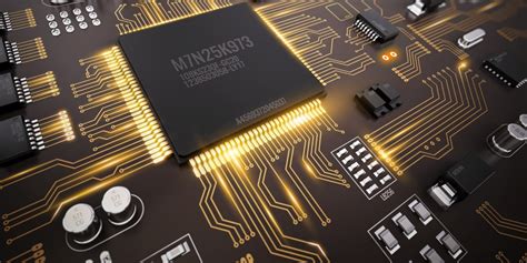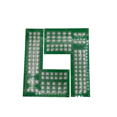
High speed signals pcb
High-speed signal PCBs are printed circuit boards that are designed to transmit high-frequency signals with minimal distortion and attenuation.
These PCBs are commonly used in electronic devices such as computers, smartphones, and networking equipment,
where high-speed data transfer is essential.
High-speed signal PCBs are typically made with specialized materials and manufacturing techniques to ensure that they can handle the high-frequency signals without introducing noise or signal loss.
They may also include features such as impedance matching, controlled routing, and shielding to further optimize signal integrity.

High-speed signals on a PCB refer to signals that operate at frequencies above a certain threshold,
typically in the range of hundreds of megahertz to several gigahertz.
These signals are often found in high-speed digital and analog circuits such as microprocessors, memory modules, and communication systems.
Designing a PCB for high-speed signals requires careful consideration of several factors,
including signal integrity, impedance control, and noise reduction.
The PCB layout should be optimized to minimize signal reflections, crosstalk, and electromagnetic interference (EMI).
This can be achieved by using controlled impedance routing, ground planes, and shielding.
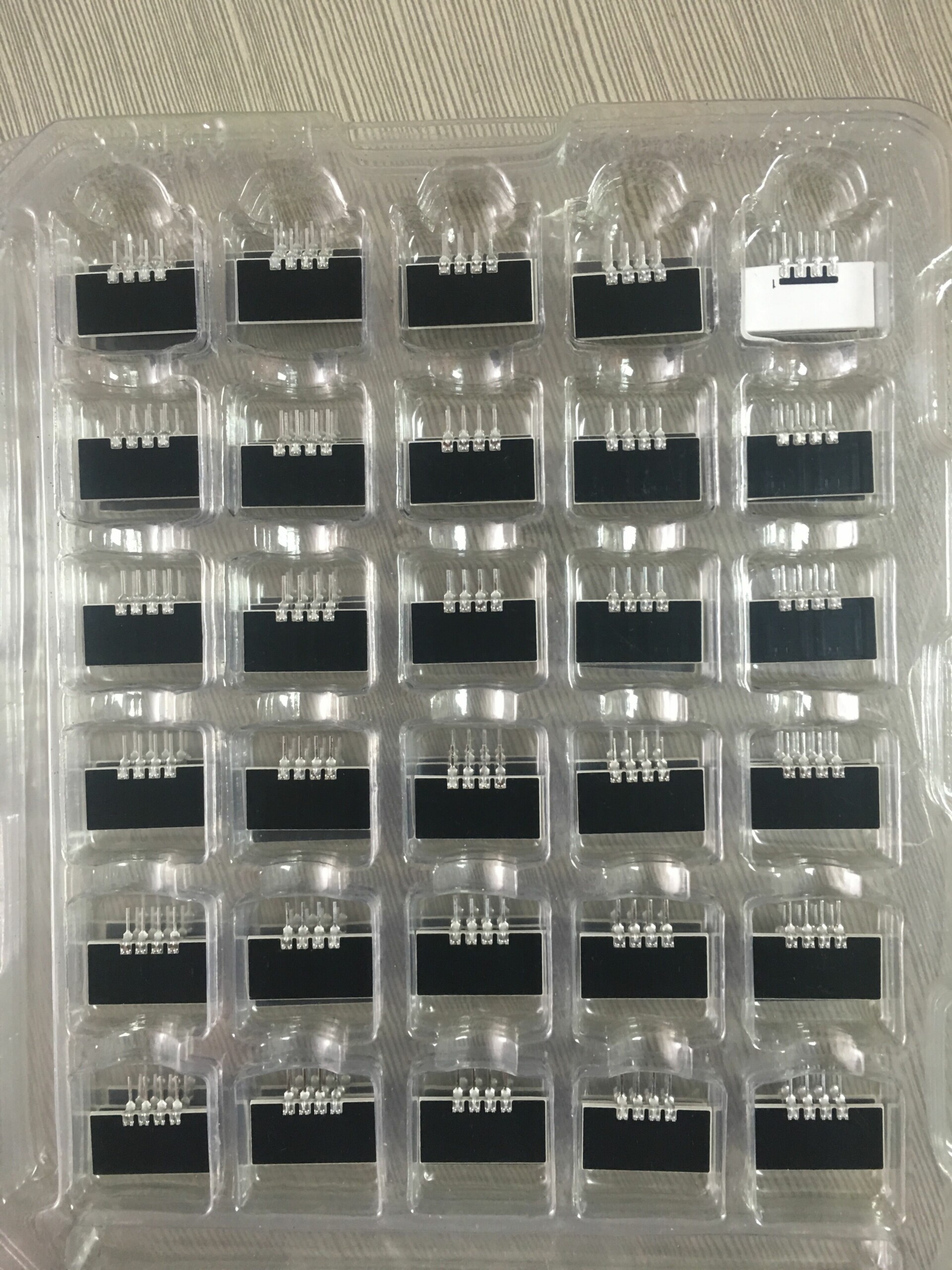
In addition, high-speed signals require special components such as high-speed connectors,
transmission lines, and signal conditioning circuits to ensure proper signal transmission and reception.
These components should be carefully selected and placed on the PCB to minimize signal distortion and attenuation.
Overall, designing a PCB for high-speed signals is a complex process that requires expertise in signal integrity,
PCB layout, and component selection. A well-designed high-speed PCB can help to ensure reliable and high-performance operation of electronic systems.

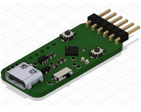
high speed signal pcb layout
High-speed signal PCB layout is a critical aspect of designing a printed circuit board that can effectively transmit high-frequency signals.
Here are some key considerations for high-speed signal PCB layout:
1. Signal Integrity:
Maintaining signal integrity is crucial for high-speed signal PCB layout.
This involves minimizing signal reflections, crosstalk, and electromagnetic interference (EMI).
To achieve this, it is important to use controlled impedance routing, proper ground and power planes, and signal shielding.
2. Component Placement:
Component placement plays a significant role in high-speed signal PCB layout.
Placing components too close together can lead to crosstalk and EMI, while placing them too far apart can increase signal loss.
It is important to place components in a way that minimizes signal path length and reduces the number of vias.
3. Routing:
Routing high-speed signals requires careful attention to detail.
Signal traces should be kept as short as possible and should avoid sharp bends or right angles.
Differential pairs should be routed together and kept parallel to minimize crosstalk.
It is also important to use vias sparingly, as each via can introduce additional signal loss and impedance changes.
4. Grounding:
Proper grounding is essential for high-speed signal PCB layout.
A solid ground plane should be used to provide a low-impedance return path for signals.
Ground vias should be placed close to signal vias to minimize loop area and reduce EMI.
5. Power Delivery:
High-speed signals require clean and stable power delivery.
Decoupling capacitors should be placed close to power pins to filter out noise and provide a stable power supply.
Power planes should be designed to minimize impedance changes and provide a low-impedance power delivery network.
In summary, high-speed signal PCB layout requires careful attention to signal integrity, component placement, routing, grounding, and power delivery.
By following these guidelines, designers can create PCBs that can effectively transmit high-frequency signals with minimal distortion and attenuation.

high speed pcb training purpose
The purpose of high speed PCB training is to provide individuals with the knowledge and skills necessary to design and develop high-speed printed circuit boards.
This includes understanding the principles of signal integrity, power integrity, electromagnetic interference (EMI),
and electromagnetic compatibility (EMC) in high-speed PCBs.
The training also covers the use of high-speed design tools, simulation software, and testing techniques to ensure the reliability and performance of the PCB.
Overall, the goal of high-speed PCB training is to equip individuals with the expertise needed to design and implement high-speed PCBs that meet the requirements of modern electronic devices and systems.