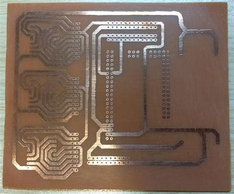
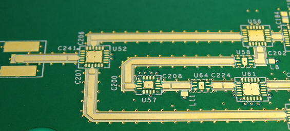
High speed usb pcb design
Optimizing Trace Widths for High-Speed USB PCB Design
In the realm of high-speed USB PCB design, optimizing trace widths is a critical factor that significantly influences the performance and reliability of the final product. As USB technology continues to evolve, with speeds reaching up to 10 Gbps and beyond, the importance of meticulous trace width optimization cannot be overstated. This process involves a careful balance of electrical, thermal, and mechanical considerations to ensure signal integrity and minimize potential issues such as crosstalk, signal loss, and electromagnetic interference (EMI).
To begin with, the electrical properties of the traces are paramount.
The characteristic impedance of a trace, which is a function of its width, height above the ground plane, and the dielectric constant of the PCB material, must be precisely controlled. For high-speed USB signals, typically operating at 90 ohms differential impedance, any deviation can lead to signal reflections and degradation. Therefore, designers must calculate the optimal trace width using impedance calculators or simulation tools, taking into account the specific stack-up configuration of the PCB.
Moreover, the thermal aspects of trace width optimization are equally important.
High-speed USB signals generate significant heat, and traces that are too narrow can exacerbate this issue, leading to potential overheating and failure. Wider traces, on the other hand, can dissipate heat more effectively, enhancing the overall thermal management of the PCB. However, excessively wide traces can introduce unwanted parasitic capacitance, which can adversely affect signal integrity. Thus, a balanced approach is necessary, where the trace width is optimized to manage heat dissipation without compromising the electrical performance.
In addition to electrical and thermal considerations, mechanical factors also play a crucial role in trace width optimization.
The mechanical strength of the traces must be sufficient to withstand the stresses of manufacturing and operational environments. Narrow traces are more susceptible to damage during the PCB fabrication process and can be prone to breaking under mechanical stress. Therefore, ensuring that the trace width is adequate to provide mechanical robustness is essential for the longevity and reliability of the high-speed USB PCB.
Transitioning from theoretical considerations to practical implementation, designers must also account for manufacturing tolerances.
PCB fabrication processes have inherent variations, and the actual trace width can differ from the designed width. To mitigate this, designers often include a margin of error in their calculations, ensuring that the final product remains within acceptable impedance and performance ranges despite these variations.
Furthermore, the layout of the PCB must be carefully planned to accommodate the optimized trace widths.
This includes maintaining consistent trace widths throughout the signal path, avoiding abrupt changes that can cause impedance discontinuities. Additionally, the routing of high-speed USB traces should minimize the length and number of vias, as these can introduce additional impedance changes and signal loss. When vias are unavoidable, their impact can be mitigated by using techniques such as back-drilling to remove unused portions of the via barrel.
In conclusion, optimizing trace widths for high-speed USB PCB design is a multifaceted process that requires a thorough understanding of electrical, thermal, and mechanical principles. By carefully balancing these factors and considering manufacturing tolerances and layout constraints, designers can achieve the desired performance and reliability for high-speed USB applications. This meticulous approach ensures that the final PCB not only meets the stringent requirements of high-speed data transmission but also maintains robustness and longevity in real-world applications.

Importance of Controlled Impedance in High-Speed USB PCB Layouts
In the realm of high-speed USB PCB design, the importance of controlled impedance cannot be overstated. As data transfer rates continue to escalate, ensuring signal integrity becomes paramount. Controlled impedance is a critical factor in maintaining the quality and reliability of high-speed signals, particularly in USB 3.0 and USB 3.1 standards, which operate at 5 Gbps and 10 Gbps respectively. The primary objective of controlled impedance is to minimize signal reflections and losses, thereby preserving the integrity of the transmitted data.
To begin with, controlled impedance refers to the characteristic impedance of a transmission line,
which is determined by the physical dimensions and material properties of the PCB traces and the surrounding dielectric. In high-speed USB designs, the differential pairs, which carry the high-speed signals, must be designed with precise impedance values, typically 90 ohms differential impedance. This precision is crucial because any deviation from the target impedance can result in signal reflections, which degrade the signal quality and can lead to data errors.
Moreover, achieving controlled impedance requires meticulous attention to the PCB stack-up and trace geometry.
The stack-up defines the arrangement of the various layers in the PCB, including the signal layers and the reference planes. By carefully selecting the dielectric materials and their thicknesses, designers can control the impedance of the traces. Additionally, the trace width and spacing must be calculated accurately to achieve the desired impedance. Tools such as impedance calculators and field solvers are often employed to assist in these calculations, ensuring that the design meets the stringent requirements of high-speed USB standards.
Transitioning to the layout phase, maintaining controlled impedance involves careful routing of the differential pairs.
It is essential to keep the differential pairs tightly coupled and to avoid any abrupt changes in trace width or spacing, which can cause impedance discontinuities. Furthermore, the length of the differential pairs should be matched as closely as possible to prevent skew, which can lead to timing issues and further degrade signal integrity. Designers must also be mindful of via placement and the use of return paths to minimize inductive and capacitive effects that can alter the impedance.
In addition to the physical design aspects, controlled impedance is also influenced by the manufacturing process.
Variations in the etching process, dielectric constant, and copper thickness can all impact the final impedance of the traces. Therefore, it is imperative to work closely with the PCB manufacturer to ensure that the design specifications are met and that any potential variations are accounted for. This collaboration helps to mitigate the risk of impedance mismatches and ensures that the final product performs as intended.
Furthermore, testing and validation play a crucial role in verifying controlled impedance in high-speed USB PCB designs.
Time-domain reflectometry (TDR) is a common technique used to measure the impedance of the traces and identify any discontinuities. By analyzing the TDR results, designers can make necessary adjustments to the layout or manufacturing process to achieve the desired impedance. This iterative process of design, manufacturing, and testing is essential to ensure the reliability and performance of high-speed USB interfaces.
In conclusion, controlled impedance is a fundamental aspect of high-speed USB PCB design that directly impacts signal integrity and data reliability. By carefully considering the PCB stack-up, trace geometry, routing practices, and manufacturing variations, designers can achieve the precise impedance required for high-speed USB standards. Through diligent testing and collaboration with manufacturers, the challenges associated with controlled impedance can be effectively managed, resulting in robust and reliable high-speed USB interfaces.
Best Practices for Ground Plane Design in High-Speed USB PCBs
In the realm of high-speed USB PCB design, the ground plane plays a pivotal role in ensuring signal integrity and minimizing electromagnetic interference (EMI). A well-designed ground plane can significantly enhance the performance and reliability of a USB circuit, particularly when dealing with high-speed data transmission. To achieve optimal results, several best practices should be adhered to during the design process.
Firstly, it is essential to maintain a continuous and unbroken ground plane.
Interruptions in the ground plane can lead to impedance discontinuities, which in turn can cause signal reflections and degrade signal quality. Therefore, designers should avoid placing vias, traces, or other components that could disrupt the continuity of the ground plane. If vias are necessary, they should be strategically placed to minimize their impact on the ground plane’s integrity.
Moreover, the placement of the ground plane relative to the signal traces is crucial.
Ideally, the ground plane should be positioned directly beneath the signal traces, providing a low-impedance return path for the high-speed signals. This configuration helps to reduce the loop area, thereby minimizing the potential for EMI. Additionally, maintaining a consistent distance between the signal traces and the ground plane is important to ensure uniform impedance, which is critical for high-speed signal transmission.
Another best practice involves the use of multiple ground planes in a multilayer PCB design.
By incorporating multiple ground planes, designers can further reduce EMI and improve signal integrity. These ground planes should be connected through an array of vias, creating a low-impedance path for return currents. This approach not only enhances the overall performance of the USB circuit but also provides better thermal management by distributing heat more evenly across the PCB.
Furthermore, careful consideration should be given to the placement of decoupling capacitors.
These capacitors are essential for filtering out high-frequency noise and providing a stable power supply to the USB components. Placing decoupling capacitors close to the power pins of the integrated circuits and connecting them directly to the ground plane can significantly improve their effectiveness. This practice helps to maintain a clean power supply, which is vital for the proper functioning of high-speed USB circuits.
In addition to these practices, designers should also pay attention to the routing of high-speed differential pairs.
Differential pairs, such as those used in USB data lines, should be routed symmetrically and with controlled impedance. The ground plane beneath these pairs should be continuous and free from any interruptions to ensure a balanced return path. This balance is crucial for minimizing common-mode noise and ensuring reliable data transmission.
Lastly, it is important to consider the overall layout of the PCB.
Components should be placed in a manner that minimizes the length of high-speed signal traces and reduces the potential for crosstalk. Grouping related components together and maintaining a clear separation between high-speed and low-speed circuits can help achieve this goal. Additionally, using ground fills or copper pours in areas where a continuous ground plane is not feasible can provide additional shielding and further reduce EMI.
In conclusion, the design of the ground plane in high-speed USB PCBs is a critical factor that directly impacts the performance and reliability of the circuit. By adhering to best practices such as maintaining a continuous ground plane, optimizing the placement of signal traces and decoupling capacitors, and carefully routing differential pairs, designers can ensure optimal signal integrity and minimize EMI. These practices, when implemented effectively, contribute to the successful design of high-speed USB PCBs that meet the stringent requirements of modern electronic devices.
Minimizing Crosstalk in High-Speed USB PCB Designs
Minimizing crosstalk in high-speed USB PCB designs is a critical aspect of ensuring signal integrity and overall system performance. As data rates increase, the potential for crosstalk—unwanted coupling of signals between adjacent traces—becomes more pronounced, leading to signal degradation and potential data errors. To address this issue, designers must employ a combination of layout strategies, material selection, and careful consideration of signal routing.
One of the primary strategies for minimizing crosstalk is to maintain adequate spacing between high-speed signal traces.
By increasing the distance between traces, the electromagnetic interference (EMI) that causes crosstalk is reduced. This can be achieved by adhering to design rules that specify minimum trace spacing based on the operating frequency and the characteristics of the PCB material. Additionally, using differential pairs for high-speed signals, such as those found in USB 3.0 and USB 3.1 standards, can help mitigate crosstalk. Differential pairs consist of two traces that carry equal and opposite signals, which helps to cancel out any noise that may be induced.
Another important consideration is the use of ground planes.
Ground planes act as a reference for signal traces and provide a low-impedance path for return currents, which helps to reduce EMI and crosstalk. Ensuring that signal traces are routed close to a continuous ground plane can significantly improve signal integrity. In multilayer PCB designs, placing high-speed signal layers adjacent to ground planes is a common practice. This not only minimizes crosstalk but also helps to control impedance, which is crucial for maintaining signal quality.
The choice of PCB material also plays a significant role in minimizing crosstalk.
High-frequency signals are more susceptible to losses and crosstalk in materials with high dielectric constants and loss tangents. Therefore, selecting low-loss materials with appropriate dielectric properties is essential for high-speed USB designs. Materials such as FR-4, while commonly used, may not always be suitable for very high-speed applications. In such cases, designers may opt for advanced materials like Rogers or Nelco laminates, which offer better performance at higher frequencies.
Signal routing techniques are equally important in minimizing crosstalk.
Avoiding parallel routing of high-speed traces over long distances can help reduce the potential for crosstalk. Instead, designers should use techniques such as serpentine routing or meandering to ensure that traces do not run parallel for extended lengths. Additionally, maintaining consistent trace widths and avoiding abrupt changes in trace direction can help maintain signal integrity.
Via placement and usage also impact crosstalk.
Vias introduce discontinuities in the signal path, which can lead to reflections and increased crosstalk. Minimizing the number of vias and ensuring that they are properly back-drilled can help mitigate these effects. When vias are necessary, placing them strategically and ensuring that they are surrounded by ground vias can help to shield high-speed signals from crosstalk.
In conclusion, minimizing crosstalk in high-speed USB PCB designs requires a comprehensive approach that includes careful consideration of trace spacing, ground plane usage, material selection, signal routing, and via placement. By implementing these strategies, designers can ensure that their high-speed USB designs maintain signal integrity and deliver reliable performance. As data rates continue to increase, the importance of addressing crosstalk in PCB design will only become more critical, making it essential for designers to stay informed about best practices and emerging technologies in this field.


