High-Tech PCB Manufacturing Excellence: Speed, Precision, Affordability

Key Takeaways
When evaluating PCB manufacturing partners, you need solutions that balance speed, precision, and PCB manufacturing cost efficiency. Leading PCB manufacturing companies leverage automated workflows and AI-driven design validation to reduce prototyping cycles by 30–50%, ensuring rapid iteration without compromising quality. For instance, modern facilities combine laser direct imaging (LDI) with advanced etching techniques to achieve micron-level accuracy—critical for high-density interconnect (HDI) boards.
| Factor | Industry Benchmark | High-Tech Advantage |
|---|---|---|
| Speed (Prototyping) | 5–7 days | 2–3 days |
| Layer Precision | ±10% tolerance | ±3% tolerance |
| Cost Optimization | Volume discounts | Dynamic pricing |
Your PCB manufacturing business decisions should prioritize vendors offering scalable production and transparent pricing models. By integrating real-time supply chain analytics, top providers mitigate material shortages and price volatility, directly impacting your project’s bottom line. Remember: PCB manufacturing isn’t just about upfront costs—it’s about securing reliability across design, fabrication, and assembly stages.
High-Tech PCB Manufacturing Innovations
At the core of modern electronics, PCB manufacturing evolves through breakthroughs like laser direct imaging (LDI) and automated optical inspection (AOI). These technologies enable micron-level accuracy in trace routing, ensuring signal integrity for high-frequency applications. Leading PCB manufacturing companies now leverage additive processes to reduce material waste, directly addressing PCB manufacturing cost challenges while maintaining performance.
Advanced substrates—such as polyimide for flexible circuits or ceramic-filled laminates for thermal management—expand design possibilities. By integrating AI-driven design validation tools, manufacturers minimize prototyping iterations, accelerating time-to-market. For businesses scaling their PCB manufacturing business, modular production lines offer adaptability to shifting demand without compromising quality.
Transitioning to Industry 4.0 standards, smart factories utilize IoT-enabled equipment for real-time process monitoring. This connectivity not only enhances precision but also strengthens supply chain resilience—a critical factor when sourcing specialized materials. Whether you require high-density interconnect (HDI) boards or multilayer configurations, these innovations ensure your projects meet both technical specifications and budgetary constraints seamlessly.
Rapid Turnkey PCB Production Solutions
When developing electronics, PCB manufacturing timelines often dictate project success. Leading PCB manufacturing companies now offer full-spectrum turnkey solutions that compress design-to-delivery cycles by integrating prototyping, component sourcing, and assembly into unified workflows. By leveraging automated quoting systems and just-in-time material procurement, you reduce PCB manufacturing cost while maintaining 48-hour rapid turnaround capabilities for prototypes and 5–7-day production for complex multilayer boards.
Advanced manufacturers deploy AI-driven design validation to preempt errors, ensuring your PCB manufacturing business avoids costly re-spins. Their digitized supply networks guarantee component availability even during shortages—critical for IoT or aerospace applications. To further accelerate timelines, cloud-based collaboration tools let you monitor production milestones in real time, synchronizing engineering adjustments across global teams.
The true value lies in balancing speed with precision: automated optical inspection (AOI) and 3D X-ray verification maintain sub-20µm alignment tolerances without delaying output. Whether scaling prototypes or managing high-mix volumes, turnkey providers optimize your time-to-market by eliminating logistical bottlenecks—proving that rapid PCB manufacturing doesn’t require compromising on quality or affordability.
Precision Engineering for Advanced PCBs
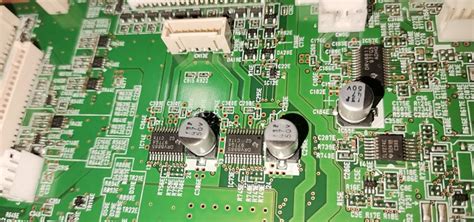
Achieving micron-level accuracy in PCB manufacturing requires more than just advanced equipment—it demands systematic expertise in material science, laser etching, and multilayer alignment. Leading PCB manufacturing companies leverage technologies like laser direct imaging (LDI) and automated optical inspection (AOI) to maintain tolerances as tight as ±0.002mm, ensuring signal integrity for high-frequency or miniaturized designs. Sub-20μm trace widths are now standard in industries like aerospace and medical devices, where reliability directly impacts performance.
"Investing in precision engineering reduces long-term PCB manufacturing cost by minimizing rework and material waste—a critical advantage for prototyping and mass production alike."
To optimize your PCB manufacturing business, prioritize suppliers with ISO 9001-certified processes and traceable quality documentation. Advanced techniques such as controlled-depth drilling and sequential lamination enable complex HDI boards while preserving cost efficiency. When selecting partners, verify their capability to handle high-density interconnect (HDI) designs and ultra-thin dielectric materials, which are essential for next-gen applications like 5G modules or IoT sensors. By balancing technical rigor with scalable workflows, you ensure both precision and affordability across your electronics projects.
Cost-Effective PCB Assembly Strategies
When optimizing pcb manufacturing cost, start by evaluating design complexity – simpler layouts using standard materials often yield substantial savings without compromising performance. Leading pcb manufacturing companies implement design-for-manufacturability (DFM) principles to eliminate unnecessary features, reducing material waste and assembly time. By partnering with suppliers offering bulk pricing for components, you secure better margins without sacrificing quality, a critical advantage in the competitive pcb manufacturing business.
Advanced panelization techniques further lower expenses by maximizing board space utilization, while automated assembly lines minimize labor costs. For prototypes or low-volume runs, modular tooling adapts existing equipment instead of requiring custom setups. However, balancing affordability with reliability requires rigorous testing protocols like automated optical inspection (AOI) and in-circuit testing (ICT), which prevent costly rework.
Transitioning to just-in-time inventory management aligns material orders with production schedules, reducing storage overhead. Many providers now offer tiered pricing models that scale with order volume, making high-quality pcb manufacturing accessible for startups and enterprises alike. This approach ensures your electronics projects stay within budget while meeting the precision demands of modern applications.
Robust Supply Chains in PCB Tech
When evaluating PCB manufacturing companies, the strength of their supply chains directly impacts your project’s success. Modern high-tech PCB production relies on seamless coordination between raw material suppliers, fabrication partners, and logistics networks. Leading manufacturers mitigate risks like material shortages or geopolitical disruptions by maintaining multi-continent supplier alliances and real-time inventory tracking systems. This ensures consistent access to specialty substrates, advanced laminates, and precision drilling tools—critical for meeting tight tolerances without inflating PCB manufacturing cost.
For businesses scaling their PCB manufacturing business, dual-sourcing strategies and vendor-managed inventory programs prove invaluable. These approaches prevent production halts while optimizing cash flow, particularly when prototyping complex HDI boards or high-volume orders. Advanced providers further integrate blockchain-enabled traceability, allowing you to verify material origins and compliance at every stage. By aligning with partners who prioritize PCB manufacturing resilience, you secure not just faster turnaround times but also long-term cost predictability—a decisive advantage in competitive electronics markets.
Quality-Driven Electronics Manufacturing
In PCB manufacturing, quality isn’t an afterthought—it’s the foundation of reliable electronics. Leading PCB manufacturing companies prioritize rigorous testing protocols, from automated optical inspection (AOI) to X-ray verification, ensuring every layer meets exacting standards. You gain assurance that your designs function as intended, even in mission-critical applications, while minimizing costly rework.
Balancing PCB manufacturing cost with quality requires strategic planning. Advanced manufacturers optimize material selection and panel utilization, reducing waste without compromising performance. For instance, partnering with firms that employ real-time process monitoring helps identify deviations early, preventing defects before they escalate. This proactive approach not only safeguards your budget but also accelerates time-to-market.
For businesses scaling their PCB manufacturing business, robust quality systems translate to long-term competitiveness. Certifications like ISO 9001 and IPC Class 3 compliance signal adherence to global benchmarks, building trust with clients. By aligning quality metrics with supply chain transparency, you ensure consistency across batches—a critical factor when delivering high-volume orders or specialized prototypes.
Ultimately, quality-driven practices elevate every stage of production, turning technical specifications into dependable end products. Whether prototyping or mass-producing, prioritizing precision at the source safeguards your investments and reinforces your reputation in fast-paced electronics markets.
Micron-Level PCB Fabrication Expertise
When developing advanced electronics, achieving micron-level precision in PCB manufacturing is non-negotiable. Leading PCB manufacturing companies leverage laser direct imaging (LDI) systems and automated optical inspection (AOI) to maintain tolerances as tight as ±25 microns, ensuring trace widths and spacing meet the demands of high-density interconnect (HDI) designs. This precision directly impacts PCB manufacturing cost by minimizing material waste and reducing rework rates—critical for balancing quality with affordability.
Modern fabrication processes incorporate advanced plating techniques and ultra-thin dielectric materials, enabling multilayer boards with consistent impedance control. Such capabilities are vital for applications like 5G infrastructure or aerospace systems, where signal integrity can’t be compromised. To stay competitive in the PCB manufacturing business, suppliers must also optimize their workflows—pairing cutting-edge equipment with rigorous testing protocols to detect defects early.
By collaborating with partners that prioritize micron-level accuracy, you secure not just functional boards, but a foundation for scalable innovation. This expertise ensures your prototypes transition seamlessly to mass production, aligning with the broader goals of speed and reliability outlined in today’s electronics landscape.
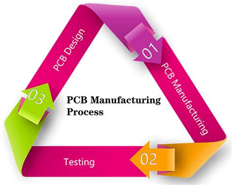
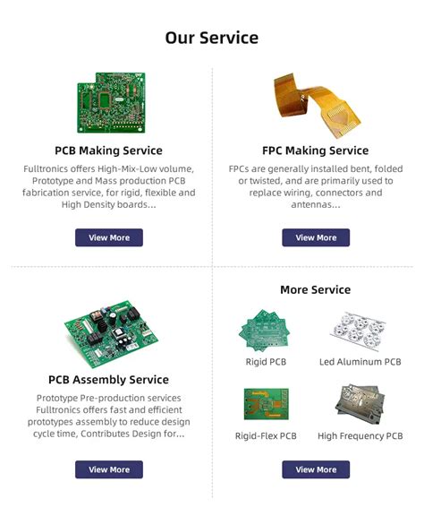
End-to-End PCB Development Services
When engaging with PCB manufacturing companies, you require more than component assembly – you need holistic solutions that bridge concept to commercialization. Leading providers now offer integrated development pipelines covering design optimization, rapid prototyping, and volume production, effectively compressing timelines while controlling PCB manufacturing cost. By collaborating with engineers from the initial schematic stage, these services identify manufacturability constraints early, preventing costly redesigns.
Advanced PCB manufacturing partners deploy simulation tools to validate thermal management and signal integrity before fabrication, ensuring compliance with industry standards like IPC-6012. Their material science expertise guides substrate selection, balancing performance requirements with budget realities – a critical advantage when scaling your PCB manufacturing business.
Transitioning seamlessly from prototype to mass production, these ecosystems leverage automated DFM (Design for Manufacturing) checks and agile supply chains to maintain consistency across batches. You gain access to real-time production analytics, enabling proactive adjustments to component sourcing or layer stack configurations. This end-to-end approach not only accelerates time-to-market but also fortifies product reliability through standardized testing protocols – from AOI (Automated Optical Inspection) to functional validation – aligning with the precision-driven demands of modern electronics.
Conclusion
When selecting PCB manufacturing partners, you need solutions that align with your project’s technical demands and budgetary constraints. Leading PCB manufacturing companies now integrate AI-driven design validation and automated optical inspection to ensure micron-level accuracy while optimizing PCB manufacturing cost. By leveraging advanced fabrication techniques like laser direct imaging and HDI stackups, these providers deliver faster prototyping cycles without compromising on reliability—a critical advantage for scaling your PCB manufacturing business.
The most competitive players combine supply chain resilience with transparent pricing models, enabling you to balance speed, precision, and affordability. Whether you’re developing IoT devices or high-frequency circuits, prioritize partners with ISO-certified PCB manufacturing workflows and real-time production tracking. This approach ensures seamless transitions from design to mass production while mitigating risks associated with component shortages or quality deviations. Ultimately, your success hinges on aligning with innovators who treat PCB manufacturing cost efficiency and technical excellence as non-negotiable pillars of service delivery.
FAQs
How quickly can PCB manufacturing companies deliver complex boards?
Most advanced providers guarantee 24-72 hour prototyping and 5-10 day full production cycles, leveraging automated workflows and just-in-time material sourcing. This ensures your project stays on schedule without compromising PCB manufacturing precision.
What factors influence PCB manufacturing cost for high-density designs?
Key determinants include layer count (8+ layers add ~15-20% per layer), surface finishes like ENIG or immersion gold (+$0.05-$0.12 per square inch), and tight tolerance requirements (<3mil trace/space). Reputable PCB manufacturing business partners provide detailed cost breakdowns upfront.
How do manufacturers ensure reliability in mission-critical applications?
Top-tier PCB manufacturing specialists implement 17+ quality checkpoints, including AOI (Automated Optical Inspection), X-ray layer alignment verification, and IPC-A-610 Class 3 compliance testing. Many combine this with real-time production tracking portals.
Can PCB manufacturing companies handle both prototype and bulk orders efficiently?
Leading providers utilize modular production lines – dedicated quick-turn cells for prototypes (<10 boards) and parallelized mass production systems for volumes up to 500,000/month. This dual approach optimizes PCB manufacturing cost across all order sizes.
What supply chain safeguards exist in modern PCB manufacturing business operations?
Proactive strategies include multi-continent material warehouses, AVL (Approved Vendor List) diversification for critical components, and blockchain-tracked raw material batches. These measures prevent 98% of potential delays in PCB manufacturing workflows.
Ready to Accelerate Your Electronics Project?
For a detailed consultation on optimizing your PCB manufacturing cost and timelines, please click here to connect with our engineering team.