High voltage pcb
Design Guidelines For High Voltage PCB Layout
Designing high voltage printed circuit boards (PCBs) requires meticulous attention to detail and adherence to specific guidelines to ensure safety, reliability, and performance. High voltage PCBs are used in various applications, including power supplies, industrial equipment, and medical devices, where the potential for electrical hazards necessitates stringent design practices. To achieve optimal results, designers must consider several critical factors, including material selection, creepage and clearance distances, and proper component placement.
One of the foremost considerations in high voltage PCB design is the selection of appropriate materials.
The dielectric properties of the substrate material play a crucial role in determining the board’s ability to withstand high voltages. Materials such as FR-4, while commonly used in standard PCBs, may not always be suitable for high voltage applications due to their limited dielectric strength. Instead, designers may opt for materials like polyimide or ceramic-filled substrates, which offer superior dielectric properties and can handle higher voltages more effectively.
In addition to material selection, maintaining adequate creepage and clearance distances is essential to prevent electrical arcing and ensure the safety of the PCB.
Creepage distance refers to the shortest path between two conductive elements along the surface of the insulating material, while clearance distance is the shortest path through the air. Both distances must be carefully calculated based on the operating voltage and environmental conditions. For instance, higher humidity levels can reduce the effectiveness of the insulating material, necessitating larger creepage and clearance distances. Adhering to industry standards, such as those outlined by the International Electrotechnical Commission (IEC), can provide valuable guidance in determining the appropriate distances for a given application.
Proper component placement is another critical aspect of high voltage PCB design.
Components that handle high voltages should be strategically placed to minimize the risk of electrical interference and arcing. For example, high voltage components should be positioned away from low voltage circuitry to prevent potential cross-talk and ensure signal integrity. Additionally, designers should consider the thermal management of high voltage components, as excessive heat can degrade the performance and reliability of the PCB. Implementing thermal vias, heat sinks, and adequate spacing between components can help dissipate heat more effectively and maintain the board’s overall performance.
Furthermore, the use of conformal coatings can enhance the safety and reliability of high voltage PCBs.
Conformal coatings provide an additional layer of insulation, protecting the board from environmental factors such as moisture, dust, and chemical contaminants. These coatings can also help increase the creepage distance by covering the surface of the PCB, thereby reducing the risk of electrical arcing. However, it is essential to select a conformal coating that is compatible with the PCB materials and application requirements to ensure optimal performance.
In conclusion, designing high voltage PCBs necessitates a comprehensive understanding of various factors, including material selection, creepage and clearance distances, component placement, and the use of conformal coatings. By adhering to established guidelines and industry standards, designers can create high voltage PCBs that are safe, reliable, and capable of withstanding the demands of their intended applications. Through careful planning and attention to detail, the challenges associated with high voltage PCB design can be effectively managed, resulting in robust and efficient electronic systems.
Safety Considerations In High Voltage PCB Design
Designing high voltage printed circuit boards (PCBs) necessitates a meticulous approach to ensure safety and reliability. High voltage applications inherently carry risks, and thus, understanding and implementing safety considerations is paramount.
One of the primary concerns in high voltage PCB design is the potential for electrical arcing, which can lead to catastrophic failures.
To mitigate this risk, designers must carefully calculate and maintain adequate spacing between conductive elements. This spacing, often referred to as creepage and clearance distances, is dictated by the voltage levels and environmental conditions in which the PCB will operate.
In addition to spacing, the choice of materials plays a crucial role in ensuring safety.
High voltage PCBs require substrates with high dielectric strength to withstand the electrical stress. Materials such as FR4, while commonly used in standard PCBs, may not always be suitable for high voltage applications. Instead, designers might opt for specialized materials like polyimide or ceramic-based substrates, which offer superior insulation properties. Furthermore, the use of conformal coatings can provide an additional layer of protection against moisture, dust, and other contaminants that could compromise the board’s integrity.
Thermal management is another critical aspect of high voltage PCB design.
High voltage components often generate significant heat, which, if not properly managed, can lead to thermal runaway and potential failure. Effective thermal management strategies include the use of heat sinks, thermal vias, and appropriate board layout techniques to dissipate heat efficiently. Additionally, designers must consider the thermal expansion properties of the materials used to prevent mechanical stress and potential damage to the PCB.
Grounding and shielding are also essential considerations in high voltage PCB design.
Proper grounding techniques help to minimize noise and interference, ensuring stable and reliable operation. Shielding, on the other hand, protects sensitive components from electromagnetic interference (EMI) and radio frequency interference (RFI), which can be particularly problematic in high voltage environments. Implementing these techniques requires a thorough understanding of the system’s electrical characteristics and careful planning during the design phase.
Moreover, safety standards and regulations must be adhered to when designing high voltage PCBs.
Various international standards, such as IPC-2221 and IEC 60950, provide guidelines on the design and manufacturing of high voltage PCBs. Compliance with these standards not only ensures the safety and reliability of the PCB but also facilitates certification and market acceptance. Designers must stay abreast of these standards and incorporate their requirements into the design process.
Testing and validation are indispensable steps in the development of high voltage PCBs.
Rigorous testing, including high potential (hipot) testing, insulation resistance testing, and thermal cycling, helps to identify potential weaknesses and ensure the board can withstand the operational stresses it will encounter. These tests provide valuable insights into the board’s performance and reliability, allowing designers to make necessary adjustments before mass production.
In conclusion, designing high voltage PCBs demands a comprehensive understanding of electrical, thermal, and mechanical principles. By carefully considering factors such as spacing, material selection, thermal management, grounding, shielding, and adherence to safety standards, designers can create robust and reliable high voltage PCBs. Rigorous testing and validation further ensure that these boards will perform safely and effectively in their intended applications. Through meticulous planning and execution, the risks associated with high voltage PCBs can be significantly mitigated, leading to safer and more reliable electronic systems.

Material Selection For High Voltage PCBs
When designing high voltage printed circuit boards (PCBs), the selection of materials is a critical factor that significantly influences the performance, reliability, and safety of the final product. High voltage PCBs are used in applications where electrical isolation, thermal management, and mechanical stability are paramount. Therefore, understanding the properties and suitability of various materials is essential for engineers and designers.
To begin with, the dielectric material used in high voltage PCBs must possess excellent insulating properties to prevent electrical breakdown and ensure reliable operation.
FR-4, a widely used material in standard PCBs, may not always be suitable for high voltage applications due to its limited dielectric strength. Instead, materials such as polyimide, PTFE (polytetrafluoroethylene), and ceramic-filled laminates are often preferred. These materials offer higher dielectric strength, better thermal stability, and improved resistance to environmental factors, making them ideal for high voltage applications.
In addition to dielectric strength, the thermal performance of the material is another crucial consideration.
High voltage circuits often generate significant amounts of heat, which must be effectively dissipated to maintain the integrity of the PCB and prevent component failure. Materials with high thermal conductivity, such as metal-core PCBs or those with ceramic substrates, are advantageous in such scenarios. These materials facilitate efficient heat dissipation, thereby enhancing the overall thermal management of the PCB.
Furthermore, the mechanical properties of the chosen material play a vital role in the durability and longevity of high voltage PCBs.
Materials that exhibit high tensile strength, low moisture absorption, and resistance to thermal cycling are preferred. For instance, polyimide materials are known for their excellent mechanical properties and can withstand harsh environmental conditions, making them suitable for high voltage applications in demanding industries such as aerospace and automotive.
Another important aspect to consider is the material’s compatibility with the manufacturing processes.
High voltage PCBs often require specialized fabrication techniques, such as thicker copper layers, wider spacing between conductors, and additional insulation layers. Therefore, the selected material must be compatible with these processes to ensure the PCB can be manufactured to the required specifications without compromising quality or performance.
Moreover, the cost and availability of materials are practical considerations that cannot be overlooked.
While high-performance materials like PTFE and ceramic-filled laminates offer superior properties, they can be significantly more expensive than standard FR-4. Balancing performance requirements with budget constraints is a common challenge faced by designers. In some cases, a hybrid approach, combining different materials within a single PCB, may be employed to optimize both performance and cost.
In conclusion, the selection of materials for high voltage PCBs is a multifaceted decision that requires careful consideration of dielectric properties, thermal performance, mechanical strength, manufacturing compatibility, and cost. By thoroughly evaluating these factors, designers can ensure that the chosen materials will meet the stringent demands of high voltage applications, resulting in reliable, efficient, and safe PCBs. As technology continues to advance, ongoing research and development in material science will likely yield new options, further enhancing the capabilities and performance of high voltage PCBs in the future.

Common Challenges In High Voltage PCB Manufacturing
High voltage printed circuit boards (PCBs) are integral components in various high-power applications, including power supplies, electric vehicles, and industrial equipment. However, manufacturing these specialized PCBs presents a unique set of challenges that must be meticulously addressed to ensure reliability and safety
. One of the primary challenges in high voltage PCB manufacturing is the need for precise material selection.
The dielectric properties of the substrate material are crucial, as they must withstand high voltages without breaking down. Materials such as FR4, while commonly used in standard PCBs, may not always be suitable for high voltage applications. Instead, manufacturers often opt for materials with higher dielectric strength, such as polyimide or ceramic-based substrates, to ensure the board can handle the electrical stress.
Another significant challenge is maintaining adequate spacing between conductive elements.
High voltage applications require larger clearance and creepage distances to prevent arcing and ensure electrical isolation. This necessitates careful design considerations and adherence to stringent industry standards, such as those outlined by the IPC-2221 guidelines. The increased spacing can also impact the overall size of the PCB, potentially leading to larger and more cumbersome designs. Consequently, designers must strike a balance between maintaining safety margins and optimizing the board’s footprint.
Thermal management is another critical aspect that cannot be overlooked.
High voltage PCBs often operate under conditions that generate substantial heat, which can degrade the board’s performance and longevity. Effective thermal management strategies, such as the incorporation of thermal vias, heat sinks, and appropriate trace widths, are essential to dissipate heat efficiently. Additionally, selecting materials with high thermal conductivity can further enhance heat dissipation, thereby improving the board’s reliability.
The manufacturing process itself poses several challenges, particularly in terms of ensuring consistent quality and reliability
. High voltage PCBs require meticulous attention to detail during fabrication, including precise drilling, plating, and etching processes. Any defects, such as voids in the plating or misalignment of layers, can compromise the board’s integrity and lead to catastrophic failures. Therefore, rigorous quality control measures, including automated optical inspection (AOI) and electrical testing, are imperative to identify and rectify any issues early in the production process.
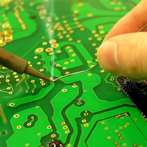
Furthermore, the assembly of high voltage PCBs demands specialized techniques and materials.
For instance, soldering processes must be carefully controlled to prevent the formation of weak joints that could fail under high voltage conditions. The use of high-temperature solder and flux materials can help achieve robust connections. Additionally, conformal coatings are often applied to high voltage PCBs to provide an extra layer of insulation and protection against environmental factors such as moisture and dust.
In conclusion, the manufacturing of high voltage PCBs is fraught with challenges that require a comprehensive understanding of materials, design principles, thermal management, and stringent quality control measures. By addressing these challenges with meticulous planning and execution, manufacturers can produce high voltage PCBs that meet the demanding requirements of high-power applications, ensuring both performance and safety.


