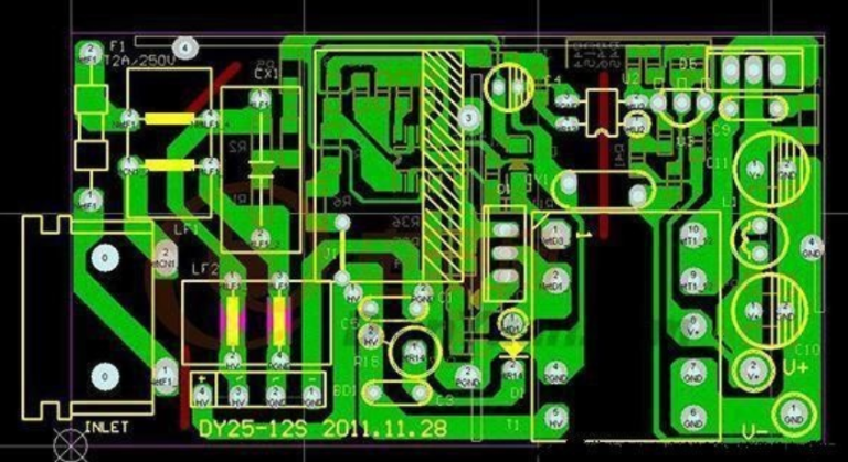
High voltage pcb design
Importance Of Clearance And Creepage In High Voltage PCB Design
In the realm of high voltage printed circuit board (PCB) design, the concepts of clearance and creepage are of paramount importance. These two parameters are critical in ensuring the safety, reliability, and performance of electronic devices that operate under high voltage conditions. Understanding and implementing appropriate clearance and creepage distances can prevent electrical failures, reduce the risk of arcing, and enhance the overall durability of the PCB.
Clearance refers to the shortest distance through the air between two conductive parts.
In high voltage applications, maintaining adequate clearance is essential to prevent electrical arcing, which can occur when the voltage difference between two conductors is sufficient to ionize the air and create a conductive path.
This phenomenon can lead to catastrophic failures, including short circuits and component damage. Therefore, designers must carefully calculate the required clearance based on the operating voltage, environmental conditions, and applicable safety standards. By adhering to these guidelines, the risk of arcing can be significantly minimized, ensuring the safe operation of the device.
Creepage, on the other hand, is the shortest path between two conductive parts along the surface of an insulating material.
Unlike clearance, which deals with air gaps, creepage considers the potential for current to travel across the surface of the PCB. This is particularly important in high voltage designs, as contaminants such as dust, moisture, and other pollutants can accumulate on the board’s surface, reducing its insulating properties. To mitigate this risk, designers must ensure that the creepage distance is sufficient to prevent surface tracking and potential short circuits. The required creepage distance is influenced by factors such as the material properties of the PCB, the level of pollution in the operating environment, and the voltage levels involved.
The importance of clearance and creepage in high voltage PCB design cannot be overstated.
These parameters are not only crucial for preventing electrical failures but also play a significant role in meeting regulatory standards and certifications. Various international standards, such as the IEC 60950-1 and IPC-2221, provide guidelines for determining the appropriate clearance and creepage distances based on specific application requirements. Compliance with these standards is essential for ensuring the safety and reliability of electronic devices, particularly in industries where high voltage applications are prevalent, such as telecommunications, power distribution, and industrial automation.
Moreover, the integration of clearance and creepage considerations into the design process can lead to more efficient and cost-effective manufacturing.
By optimizing these distances, designers can reduce the size of the PCB, leading to material savings and potentially lower production costs. Additionally, a well-designed PCB with adequate clearance and creepage can enhance the longevity of the device, reducing the likelihood of costly repairs or replacements due to electrical failures.
In conclusion, clearance and creepage are fundamental aspects of high voltage PCB design that directly impact the safety, performance, and compliance of electronic devices. By understanding and implementing these parameters effectively, designers can ensure that their products operate reliably under high voltage conditions, meet regulatory requirements, and provide long-term value to end-users. As technology continues to advance and the demand for high voltage applications grows, the importance of these design considerations will only become more pronounced, underscoring the need for meticulous attention to detail in the PCB design process.
Material Selection For High Voltage PCB Applications
In the realm of high voltage PCB design, the selection of appropriate materials is a critical factor that significantly influences the performance, reliability, and safety of the final product. As electronic devices continue to evolve, the demand for high voltage applications has increased, necessitating a deeper understanding of the materials that can withstand such conditions. The choice of materials is not merely a matter of selecting components that can handle high voltages; it involves a comprehensive evaluation of various properties that contribute to the overall functionality and durability of the PCB.
To begin with, dielectric strength is a paramount consideration in high voltage PCB applications.
This property determines the material’s ability to resist electrical breakdown when subjected to high voltages. Materials with high dielectric strength are essential to prevent arcing and ensure the integrity of the circuit. Common materials such as FR-4, while widely used in standard PCBs, may not always suffice for high voltage applications due to their limited dielectric strength. Therefore, alternatives like polyimide or ceramic-based substrates are often preferred, as they offer superior dielectric properties.
In addition to dielectric strength, thermal performance is another crucial factor.
High voltage applications often generate significant amounts of heat, which can lead to thermal stress and potential failure if not properly managed. Materials with high thermal conductivity are advantageous as they facilitate efficient heat dissipation, thereby maintaining the stability of the PCB. For instance, metal-core PCBs, which incorporate a metal layer to enhance thermal management, are frequently employed in high voltage designs to address this challenge.
Moreover, the coefficient of thermal expansion (CTE) is an important consideration when selecting materials for high voltage PCBs.
A mismatch in CTE between the substrate and other components can lead to mechanical stress and eventual failure, especially under thermal cycling conditions. Therefore, materials with a CTE that closely matches that of the components are preferred to ensure mechanical stability and longevity.
Furthermore, moisture absorption is a factor that cannot be overlooked in high voltage PCB material selection.
Moisture can significantly degrade the dielectric properties of a material, leading to reduced performance and increased risk of electrical failure. Consequently, materials with low moisture absorption rates are ideal for high voltage applications, as they maintain their electrical properties even in humid environments.
Additionally, chemical resistance is a consideration that ensures the longevity and reliability of high voltage PCBs.
Exposure to harsh chemicals or environmental conditions can compromise the integrity of the PCB material, leading to potential failures. Therefore, selecting materials that exhibit strong chemical resistance is essential for applications where such exposure is likely.
In conclusion, the selection of materials for high voltage PCB applications is a multifaceted process that requires careful consideration of various properties, including dielectric strength, thermal performance, CTE, moisture absorption, and chemical resistance. By prioritizing these factors, designers can ensure that their high voltage PCBs not only meet the necessary performance standards but also provide long-term reliability and safety. As technology continues to advance, the development of new materials with enhanced properties will undoubtedly play a pivotal role in the evolution of high voltage PCB design, enabling more efficient and robust electronic solutions.
Techniques For Minimizing Electromagnetic Interference In High Voltage PCBs
In the realm of high voltage printed circuit board (PCB) design, minimizing electromagnetic interference (EMI) is a critical consideration that ensures both the functionality and reliability of electronic systems. As electronic devices become increasingly complex, the potential for EMI to disrupt operations grows, necessitating the implementation of effective techniques to mitigate its impact. Understanding the sources and pathways of EMI is the first step in developing strategies to minimize its effects in high voltage PCBs.
One fundamental technique for reducing EMI is the careful layout of the PCB.
The physical arrangement of components and traces can significantly influence the electromagnetic compatibility of the board. By strategically placing components and routing traces, designers can minimize loop areas, which are potential sources of radiated emissions. Additionally, maintaining a consistent ground plane across the PCB can help reduce the impedance of return paths, thereby minimizing the potential for EMI.
Moreover, the use of differential signaling is another effective method for minimizing EMI in high voltage PCBs.
Differential signaling involves transmitting signals using two complementary voltage levels, which can help cancel out noise and reduce electromagnetic emissions. This technique is particularly useful in high-speed applications where signal integrity is paramount. By employing differential pairs and ensuring that they are routed closely together, designers can further enhance the board’s resistance to EMI.
In addition to layout considerations, the selection of appropriate materials plays a crucial role in EMI mitigation.
High-quality dielectric materials with low loss tangents can help reduce signal attenuation and minimize the potential for EMI. Furthermore, the use of shielding materials, such as copper or aluminum, can provide an additional layer of protection against electromagnetic interference. These materials can be applied as a coating or integrated into the PCB design to create a Faraday cage effect, effectively blocking external electromagnetic fields.
Another technique involves the implementation of filtering components, such as ferrite beads and capacitors, which can suppress high-frequency noise and prevent it from propagating through the circuit.
Ferrite beads, in particular, are effective at attenuating high-frequency signals while allowing low-frequency signals to pass through. By strategically placing these components at key points in the circuit, designers can significantly reduce the impact of EMI on the overall system performance.
Furthermore, the use of proper grounding techniques is essential in minimizing EMI in high voltage PCBs.
A well-designed grounding scheme can help dissipate unwanted electromagnetic energy and prevent it from affecting sensitive components. Techniques such as star grounding, where all ground connections converge at a single point, can help minimize ground loops and reduce the potential for EMI.
Finally, simulation and testing are indispensable tools in the process of minimizing EMI in high voltage PCB design.
By utilizing electromagnetic simulation software, designers can predict potential EMI issues and evaluate the effectiveness of various mitigation strategies before physical prototyping. Additionally, thorough testing in anechoic chambers or using spectrum analyzers can help identify and address any residual EMI concerns, ensuring that the final product meets regulatory standards and performs reliably in real-world conditions.
In conclusion, minimizing electromagnetic interference in high voltage PCB design requires a multifaceted approach that encompasses careful layout, material selection, filtering, grounding, and rigorous testing. By employing these techniques, designers can enhance the electromagnetic compatibility of their PCBs, ensuring that they operate efficiently and reliably in increasingly complex electronic environments.
Thermal Management Strategies In High Voltage PCB Design
In the realm of high voltage PCB (Printed Circuit Board) design, thermal management emerges as a critical consideration, given the potential for excessive heat generation that can compromise both performance and safety. As electronic devices become increasingly compact and powerful, the need for effective thermal management strategies becomes paramount. High voltage PCBs, in particular, are susceptible to thermal issues due to the high power levels they handle, which can lead to elevated temperatures and, consequently, thermal stress. Therefore, understanding and implementing effective thermal management strategies is essential for ensuring the reliability and longevity of these systems.
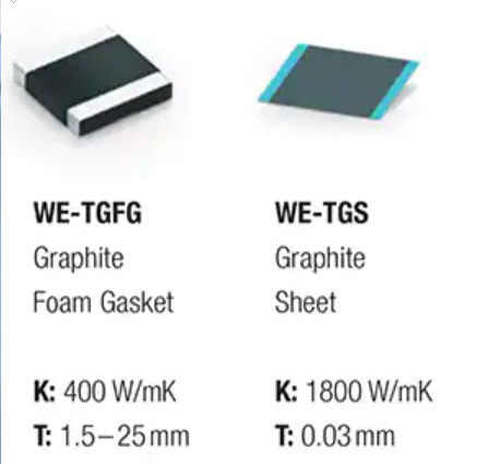
To begin with, one of the primary strategies in thermal management is the selection of appropriate materials.
The choice of substrate material can significantly influence the thermal performance of a high voltage PCB. Materials with high thermal conductivity, such as aluminum or copper, are often preferred as they facilitate efficient heat dissipation. Additionally, the use of thermal interface materials (TIMs) can enhance the thermal connection between components and heat sinks, further aiding in heat transfer.
Moreover, the design layout plays a crucial role in thermal management.
Strategic placement of components can minimize thermal hotspots and ensure even heat distribution across the PCB. For instance, high-power components should be positioned away from heat-sensitive areas, and adequate spacing should be maintained to allow for effective heat dissipation. Furthermore, incorporating thermal vias—small holes filled with conductive material—can help transfer heat from the surface of the PCB to the inner layers or to an external heat sink, thereby reducing surface temperature.
In addition to material selection and layout considerations, active cooling methods can be employed to manage thermal challenges in high voltage PCBs.
These methods include the use of fans or liquid cooling systems to actively remove heat from the board. While these solutions can be effective, they also introduce additional complexity and cost, making them more suitable for applications where passive cooling methods are insufficient.
Another important aspect of thermal management is the use of simulation tools during the design phase.
Thermal simulation software allows designers to model the thermal behavior of a PCB under various operating conditions. By predicting potential thermal issues before physical prototypes are built, designers can make informed decisions about material selection, component placement, and cooling strategies. This proactive approach not only saves time and resources but also enhances the overall reliability of the final product.
Furthermore, it is essential to consider the impact of environmental factors on thermal performance.
High voltage PCBs may be subjected to varying ambient temperatures, humidity levels, and airflow conditions, all of which can influence heat dissipation. Designing for worst-case scenarios ensures that the PCB can operate safely and efficiently under all expected conditions. This may involve incorporating additional thermal management features or selecting components with higher temperature ratings.
In conclusion, effective thermal management in high voltage PCB design is a multifaceted challenge that requires careful consideration of materials, layout, cooling methods, and environmental factors. By employing a combination of these strategies, designers can mitigate thermal risks and enhance the performance and reliability of high voltage PCBs. As technology continues to advance, the importance of robust thermal management will only grow, underscoring the need for ongoing innovation and adaptation in this critical area of electronic design.