How do pcb boards work
Understanding how do pcb boards work
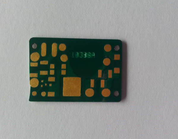
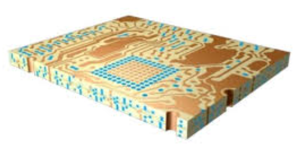
Printed Circuit Boards (PCBs) are the backbone of modern electronic devices, serving as the foundation upon which electronic components are mounted and interconnected. To understand how PCB boards work, it is essential to delve into their structure, materials, and the principles that govern their operation. At the most fundamental level, a PCB is a flat, rigid board made from a non-conductive substrate, typically fiberglass, which provides mechanical support and insulation for the conductive pathways etched onto its surface.
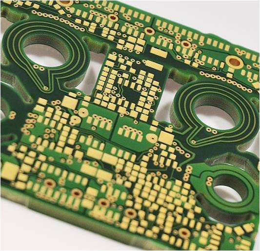
The conductive pathways, or traces, are made of copper and are meticulously designed to create electrical connections between various components.
These traces are formed through a process called photolithography, where a photoresist material is applied to the copper-clad board, exposed to ultraviolet light through a mask, and then developed to reveal the desired pattern. The exposed copper is subsequently etched away, leaving behind the intricate network of traces that define the circuit.
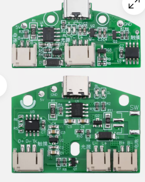
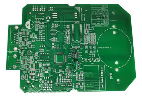
Components such as resistors, capacitors, diodes, and integrated circuits are then soldered onto the PCB. Soldering involves melting a metal alloy, typically composed of tin and lead or a lead-free alternative, to create a strong electrical and mechanical bond between the component leads and the copper traces. This process ensures that the components are securely attached and can effectively transmit electrical signals.
One of the key advantages of PCBs is their ability to support complex circuits in a compact and organized manner.
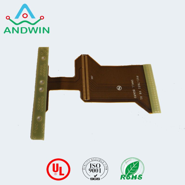
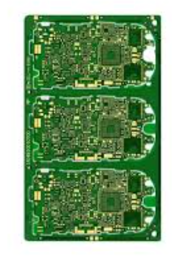
This is achieved through the use of multiple layers, which can be stacked to create multilayer PCBs. Each layer consists of its own set of traces and is separated by insulating material. Vias, which are small holes drilled through the board and plated with conductive material, allow for electrical connections between different layers. This multilayer approach enables the design of highly sophisticated circuits with minimal space requirements.
The functionality of a PCB is determined by the arrangement and interconnection of its components.
When an electrical signal is introduced into the circuit, it travels along the copper traces, passing through various components that modify the signal in specific ways. For instance, resistors limit the flow of current, capacitors store and release electrical energy, and diodes allow current to flow in only one direction. Integrated circuits, which are essentially miniature electronic circuits encapsulated in a single package, perform more complex functions such as amplification, signal processing, and computation.
To ensure the reliability and performance of a PCB, designers must carefully consider factors such as trace width, spacing, and the placement of components.
These considerations are crucial for preventing issues such as signal interference, crosstalk, and overheating. Additionally, PCBs often incorporate ground planes and power planes, which are large areas of copper that provide stable reference voltages and help dissipate heat.
In conclusion, PCB boards are integral to the operation of modern electronic devices, providing a structured and efficient means of interconnecting components. Their design and fabrication involve a combination of materials science, electrical engineering, and precision manufacturing techniques. By understanding the basics of PCB boards, one gains insight into the intricate processes that enable the functionality of countless electronic systems that permeate our daily lives.
The Role Of Copper Traces In PCB Functionality
Printed Circuit Boards (PCBs) are the backbone of modern electronic devices, providing a platform for mounting and interconnecting various electronic components. Central to the functionality of PCBs are copper traces, which play a crucial role in ensuring the efficient operation of electronic circuits. Understanding the role of copper traces in PCB functionality requires a closer examination of their design, purpose, and impact on the overall performance of electronic devices.
Copper traces are thin lines of copper that are etched onto the surface of a PCB.
These traces act as conductive pathways, allowing electrical signals to travel between different components on the board. The process of creating these traces involves several steps, starting with the application of a copper layer onto a non-conductive substrate, typically made of fiberglass or other insulating materials. This copper layer is then selectively etched away using a chemical process, leaving behind the desired pattern of traces.
The primary function of copper traces is to provide a reliable and efficient means of electrical connectivity.
By serving as conduits for electrical signals, these traces enable the various components on a PCB to communicate and work together harmoniously. For instance, in a simple circuit, copper traces might connect a power source to a microcontroller, which in turn is connected to sensors and output devices. The integrity and design of these traces are paramount, as any disruption or flaw can lead to signal loss, interference, or even complete circuit failure.
Moreover, the width and thickness of copper traces are critical factors that influence their performance.
Thicker and wider traces can carry higher currents without overheating, which is essential for power distribution within the PCB. Conversely, thinner traces are suitable for low-current signal transmission but must be carefully designed to avoid issues such as signal degradation or electromagnetic interference. Engineers must balance these considerations to ensure that the PCB meets the specific requirements of the application it is intended for.
In addition to their role in signal transmission, copper traces also contribute to the thermal management of PCBs.
Electronic components generate heat during operation, and efficient heat dissipation is crucial to maintaining the reliability and longevity of the device. Copper traces can help distribute heat away from critical components, preventing localized hotspots and reducing the risk of thermal damage. This is particularly important in high-power applications, where effective thermal management is essential to prevent overheating and ensure stable performance.
Furthermore, the layout and routing of copper traces are vital aspects of PCB design.
Proper routing minimizes the length of signal paths, reducing the potential for signal delay and ensuring faster communication between components. Additionally, careful layout planning can help mitigate issues such as crosstalk, where signals in adjacent traces interfere with each other, leading to data corruption or erratic behavior. Advanced design techniques, such as differential pair routing and controlled impedance traces, are often employed to enhance signal integrity and overall PCB performance.
In conclusion, copper traces are indispensable elements of PCB functionality, serving as the lifelines that connect and enable the operation of electronic components. Their design, width, thickness, and routing all play critical roles in ensuring efficient electrical connectivity, effective thermal management, and reliable signal transmission. As technology continues to advance, the importance of well-designed copper traces in the development of sophisticated electronic devices cannot be overstated. Understanding and optimizing these traces is essential for engineers striving to create high-performance, reliable, and efficient PCBs.
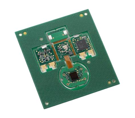
How Components Are Mounted On PCB Boards
Printed Circuit Boards (PCBs) serve as the backbone of modern electronic devices, providing a platform for mounting and interconnecting various electronic components. Understanding how components are mounted on PCB boards is crucial for comprehending the functionality and reliability of electronic systems. The process of mounting components on PCBs involves several meticulous steps, each contributing to the overall performance and durability of the final product.
Initially, the design phase plays a pivotal role in determining how components will be mounted on the PCB.
Engineers use specialized software to create a schematic diagram, which outlines the electrical connections and placements of components. This schematic is then translated into a layout design, specifying the exact locations where components will be mounted. The layout design ensures that components are optimally placed to minimize signal interference and maximize efficiency.
Once the design is finalized, the actual mounting process begins with the preparation of the PCB.
The board is typically made from a non-conductive substrate, such as fiberglass, coated with a thin layer of conductive material, usually copper. This copper layer is etched to create the circuit pattern, which will connect the various components. The board is then cleaned to remove any contaminants that could affect the soldering process.
The next step involves the application of solder paste to the PCB.
Solder paste is a mixture of tiny solder balls and flux, which helps the solder to flow and adhere to the components and the board. The paste is applied to the board using a stencil, which ensures that it is only deposited on the areas where components will be mounted. This precise application is crucial for preventing solder bridges and ensuring reliable connections.
Following the application of solder paste, the components are placed on the PCB.
This is typically done using automated machines known as pick-and-place machines. These machines are programmed to pick up components from reels or trays and place them accurately on the board. The use of automation ensures high precision and consistency, which is essential for the functionality of the final product.
After the components are placed, the PCB undergoes a reflow soldering process.
During reflow soldering, the board is passed through an oven where it is gradually heated to a temperature that melts the solder paste. As the solder melts, it forms a strong electrical and mechanical bond between the components and the PCB. The board is then cooled, solidifying the solder and securing the components in place.
In addition to reflow soldering, some components may require through-hole mounting, especially those that need to handle higher currents or mechanical stress. Through-hole components have leads that pass through holes in the PCB and are soldered on the opposite side. This method provides a more robust mechanical connection but is generally more labor-intensive and less suitable for high-density designs.
Once all components are mounted and soldered, the PCB undergoes inspection and testing to ensure that it functions correctly. Automated optical inspection (AOI) systems are used to check for soldering defects, misaligned components, and other issues. Functional testing is also performed to verify that the PCB operates as intended.
In conclusion, the process of mounting components on PCB boards involves a series of carefully orchestrated steps, from design and preparation to soldering and inspection. Each step is critical to ensuring the reliability and performance of the final electronic product. By understanding these processes, one gains a deeper appreciation for the complexity and precision involved in modern electronics manufacturing.
The Importance Of PCB Design In Circuit Performance
Printed Circuit Boards (PCBs) are the backbone of modern electronic devices, serving as the foundation upon which all other components are mounted. The importance of PCB design in circuit performance cannot be overstated, as it directly influences the functionality, reliability, and efficiency of the final product. To understand the significance of PCB design, it is essential to delve into the intricacies of how these boards work and the factors that contribute to their optimal performance.
At its core, a PCB is a flat, insulating board made of materials such as fiberglass or composite epoxy, onto which conductive pathways are etched or printed.
These pathways, often made of copper, form the electrical connections between various components, such as resistors, capacitors, and integrated circuits. The layout of these pathways is meticulously designed to ensure that electrical signals travel efficiently and without interference, which is crucial for the proper functioning of the circuit.
One of the primary considerations in PCB design is the arrangement of components.
Proper placement is vital to minimize signal interference and ensure efficient heat dissipation. Components that generate significant heat, such as power transistors and voltage regulators, must be strategically positioned to prevent overheating and potential damage to the board. Additionally, the proximity of components that interact frequently can reduce the length of conductive pathways, thereby minimizing signal delay and power loss.
Another critical aspect of PCB design is the routing of traces, which are the conductive pathways that connect different components.
The width and length of these traces must be carefully calculated to handle the required current without excessive resistance or heat generation. Moreover, the routing must avoid creating loops or crossing paths that could lead to electromagnetic interference (EMI). To mitigate EMI, designers often employ techniques such as grounding planes and shielding, which help to isolate sensitive signals from potential sources of noise.
The choice of materials also plays a significant role in PCB performance.
High-frequency circuits, for instance, require materials with low dielectric loss to maintain signal integrity. Similarly, the thermal properties of the substrate material can impact the board’s ability to dissipate heat, which is crucial for maintaining the longevity and reliability of the components. Advanced PCBs may incorporate multiple layers, each serving a specific purpose, such as power distribution, signal routing, or grounding. These multilayer boards offer greater design flexibility and can accommodate more complex circuits within a compact form factor.
Furthermore, the manufacturing process of PCBs must adhere to stringent quality standards to ensure consistent performance.
Precision in etching, drilling, and soldering is paramount to avoid defects such as short circuits, open circuits, or misaligned components. Automated testing procedures, such as in-circuit testing (ICT) and automated optical inspection (AOI), are employed to verify the integrity of the board before it is integrated into the final product.
In conclusion, the design of a PCB is a meticulous process that requires careful consideration of various factors, including component placement, trace routing, material selection, and manufacturing precision. Each of these elements plays a crucial role in determining the overall performance and reliability of the circuit. As electronic devices continue to evolve and become more sophisticated, the importance of PCB design in circuit performance will only grow, underscoring the need for skilled designers who can navigate the complexities of this critical field.