How Does Current Flow in a PCB? Understanding the Pathways of Electrical Current in Printed Circuit Boards
Introduction to Current Flow in PCBs
Printed Circuit Boards (PCBs) form the backbone of modern electronics, providing both mechanical support and electrical connections between components. Understanding how current flows through these intricate boards is fundamental for engineers, designers, and anyone working with electronic systems. Current flow in PCBs differs from simple wire connections due to the complex two-dimensional (and sometimes multi-layer) nature of circuit boards, the presence of various materials with different conductive properties, and the high-frequency effects that come into play with modern high-speed electronics.
At its core, electrical current in a PCB flows through conductive pathways—primarily copper traces—from power sources to components and between interconnected components. However, this simple description belies the complexity of actual current behavior in circuit boards, which involves considerations of resistance, capacitance, inductance, and electromagnetic field effects that become particularly important as signal frequencies increase and device sizes decrease.
The Physical Pathways of Current in PCBs
Copper Traces: The Primary Conductors
The most obvious pathways for current flow in a PCB are the copper traces etched onto the board’s substrate. These traces serve as the wiring of the circuit, connecting various components according to the designed schematic. Current flows through these traces much like it flows through wires, but with some important differences due to their flat, rectangular cross-section and proximity to other conductive elements.
The current-carrying capacity of a trace depends on several factors:
- Cross-sectional area (width × thickness)
- Copper weight (typically 0.5 oz/ft² to 2 oz/ft²)
- Maximum allowable temperature rise
- Ambient temperature
- Presence of adjacent traces or heat sources
Vias: Vertical Current Pathways
In multi-layer PCBs, vias provide vertical connections between layers. These plated-through holes allow current to flow from one layer of the board to another. There are several types of vias:
- Through-hole vias: Span the entire board thickness
- Blind vias: Connect an outer layer to one or more inner layers
- Buried vias: Connect only inner layers without reaching the surface
Current flow through vias is more complex than through surface traces due to their cylindrical geometry and the presence of plating material of varying thickness. Via resistance can become significant in high-current applications, and via stitching (multiple vias in parallel) is often used to reduce resistance and improve current handling capacity.
Planes: Distributed Current Flow
Power and ground planes in multi-layer PCBs provide low-impedance, distributed current pathways. Unlike traces that carry current along specific paths, planes allow current to spread out across a wide area. This has several advantages:
- Lower inductance than narrow traces
- Better heat dissipation
- Reduced voltage drop
- Improved high-frequency performance
Current in planes doesn’t follow simple linear paths—it tends to distribute itself according to the principle of least impedance, which at high frequencies may not be the geometrically shortest path between two points.
Current Flow Mechanisms and Considerations
DC Current Flow
Under direct current (DC) conditions, current flows uniformly through the entire cross-section of conductors (skin effect is negligible). The primary considerations for DC current flow are:
- Resistance: Governed by the bulk resistivity of copper and the trace dimensions
- Voltage drop: Especially important in power distribution networks
- Current density: Must remain below levels that would cause excessive heating
The resistance of a trace can be calculated using:
R = ρ × L / (W × T)
Where:
ρ = resistivity of copper (1.72×10⁻⁶ Ω·cm at 20°C)
L = trace length
W = trace width
T = trace thickness
AC Current Flow and Skin Effect
At alternating current (AC) or high-frequency signals, current flow becomes more complex due to electromagnetic effects. The skin effect causes current to concentrate near the surface of conductors, effectively reducing the usable cross-section at higher frequencies. The skin depth (δ) is given by:
δ = √(ρ / (π × μ × f))
Where:
ρ = resistivity
μ = permeability (μ₀ for copper)
f = frequency
For copper at room temperature:
δ ≈ 66 μm / √f (with f in Hz)
This means at 1 MHz, skin depth is about 66 μm—comparable to the thickness of many PCB traces. Above this frequency, current flows primarily in a thin layer near the surface, increasing effective resistance.
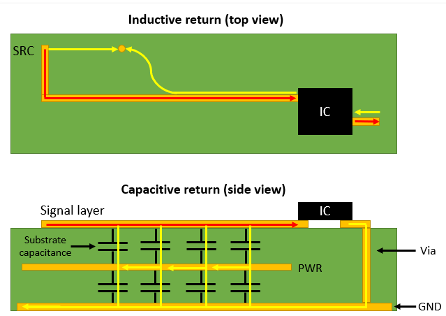
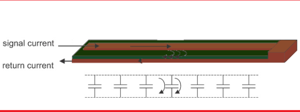
Return Current Paths
A complete circuit requires both outgoing and return current paths. In PCB design, understanding return current flow is crucial, especially for:
- Signal integrity
- Electromagnetic interference (EMI) control
- Ground bounce minimization
At DC and low frequencies, return current follows the path of least resistance, which is typically the geometrically shortest path back to the source. At high frequencies, return current follows the path of least inductance, which tends to be directly beneath the signal trace (even if this isn’t the shortest geometric path).
In multi-layer boards with ground planes, high-frequency return current flows primarily in the ground plane directly beneath the signal trace, creating a transmission line effect. This behavior is why maintaining uninterrupted reference planes is critical for high-speed design.
Current Distribution in Different PCB Configurations
Single-Layer Boards
In single-layer PCBs, all connections must be made on one side of the board, requiring more complex routing. Current flows:
- Through traces connecting components
- Through jumpers or wire bridges when traces must cross
- Via component leads where traces cannot complete connections
Return currents must often travel longer distances, potentially creating ground loops and EMI issues.
Double-Layer Boards
Two-layer boards offer more routing flexibility, typically using:
- One layer primarily for horizontal traces
- The other layer primarily for vertical traces
- Often with one layer serving as a ground or power plane
Current can take more direct paths, and return currents have lower impedance paths available.
Multi-Layer Boards
Modern high-density designs often use 4, 6, 8 or more layers with dedicated functions:
- Signal layers (for component interconnections)
- Power planes (distributing VCC and other voltages)
- Ground planes (providing low-impedance return paths)
In such boards, current flows:
- Horizontally in signal layers between components
- Vertically through vias between layers
- Distributed through planes for power distribution and return paths
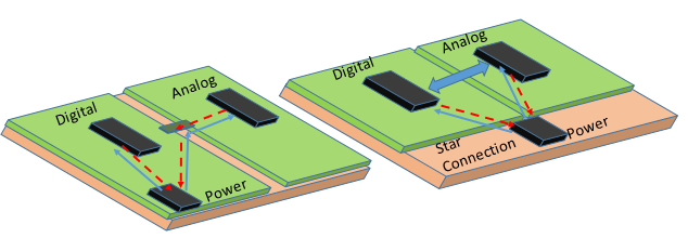
Proper stackup design ensures controlled impedance and minimizes cross-talk between signals.
Practical Considerations for PCB Current Flow
Current Density and Heating
Excessive current density leads to heating, which can:
- Change material properties (increasing resistance)
- Cause thermal expansion stresses
- Potentially damage the board or components
Design rules typically specify maximum current per trace width based on acceptable temperature rise.
High-Current Applications
For high-current paths (power supplies, motor drivers, etc.):
- Use wider traces
- Increase copper weight (thickness)
- Employ copper pours or planes
- Use multiple vias in parallel
- Consider exposed copper with additional solder or bus bars
High-Speed Design Considerations
At high frequencies (typically >50 MHz):
- Maintain uninterrupted return paths
- Control impedance by careful trace geometry
- Minimize via transitions (which cause impedance discontinuities)
- Consider differential signaling for critical paths
- Use proper termination to prevent reflections
Measuring and Analyzing Current Flow in PCBs
Simulation Tools
Modern EDA tools can simulate current flow:
- DC analysis shows steady-state current distribution
- AC analysis reveals frequency-dependent behavior
- Electromagnetic field solvers model high-frequency effects
Physical Measurement Techniques
Actual current flow can be measured using:
- Current probes (for accessible traces)
- Shunt resistors (measuring voltage drop)
- Hall effect sensors (non-contact measurement)
- Infrared thermography (indirect via heating patterns)
Conclusion
Current flow in PCBs is a complex phenomenon that ranges from simple DC conduction through copper traces to sophisticated high-frequency electromagnetic field interactions in multi-layer boards. Understanding these current pathways is essential for designing reliable, efficient, and high-performance electronic circuits. As PCB technology continues to evolve with higher densities, faster signals, and more demanding applications, the principles governing current flow remain fundamental to successful design implementation.
Good PCB layout practices account for both the intended current paths and the unintended consequences of current flow—parasitic resistances, inductive and capacitive coupling, ground bounce, and electromagnetic interference. By carefully considering how current will flow during the design phase, engineers can create circuit boards that perform reliably across all required operating conditions.