How does pcb assembly work
Understanding The Basics Of PCB Assembly
Printed Circuit Board (PCB) assembly is a critical process in the manufacturing of electronic devices, serving as the backbone for most electronic circuits. Understanding the basics of PCB assembly involves delving into the various stages and components that contribute to the creation of a functional electronic board. This process begins with the design phase, where engineers use specialized software to create a schematic diagram of the circuit. The schematic is then translated into a layout that specifies the placement of components and the routing of electrical connections.
Once the design is finalized, the next step is the fabrication of the PCB itself.
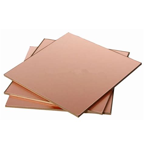
This involves creating the physical board, typically made from a non-conductive substrate such as fiberglass, with copper layers laminated onto it. The copper layers are etched to form the circuit traces, which are the pathways that will carry electrical signals between components. After etching, the board undergoes a series of cleaning and inspection processes to ensure that it meets the required specifications.
Following the fabrication of the PCB, the assembly process begins with the application of solder paste to the board.
Solder paste is a mixture of tiny solder balls and flux, which helps to clean the surfaces and improve the flow of solder. The paste is applied to the board using a stencil that masks off areas where solder is not needed. This step is crucial as it ensures that the components will be securely attached to the board.
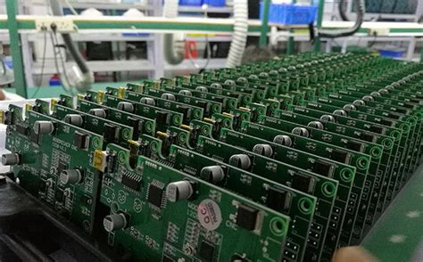
Next, the components are placed onto the board. This is typically done using automated machines known as pick-and-place machines, which can accurately position components at high speeds. These machines use a combination of vacuum nozzles and vision systems to pick up components from reels or trays and place them onto the board in the correct orientation. The accuracy of this step is vital, as even slight misalignments can lead to malfunctioning circuits.
Once all the components are in place, the board is subjected to a reflow soldering process.
During reflow soldering, the board is passed through an oven where it is gradually heated to a temperature that melts the solder paste. As the solder cools, it solidifies, forming strong electrical and mechanical connections between the components and the board. This process must be carefully controlled to prevent defects such as solder bridges or cold joints, which can compromise the functionality of the circuit.
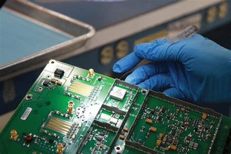
After reflow soldering, the assembled PCB undergoes a series of inspections and tests to ensure its quality and reliability.
Automated optical inspection (AOI) systems are commonly used to check for defects such as missing components, misalignments, or soldering issues. Additionally, electrical tests are performed to verify that the circuit functions as intended. These tests may include in-circuit testing (ICT), which checks the electrical performance of individual components, and functional testing, which evaluates the overall operation of the assembled board.
In conclusion, PCB assembly is a complex and precise process that involves multiple stages, from design and fabrication to component placement and soldering. Each step must be meticulously executed to ensure the production of high-quality electronic boards. Understanding the basics of PCB assembly provides valuable insight into the intricate processes that underpin modern electronic devices, highlighting the importance of precision and quality control in the manufacturing of reliable and efficient circuits.
Step-By-Step Guide To PCB Assembly Process
Printed Circuit Board (PCB) assembly is a meticulous process that involves several stages, each crucial to the creation of a functional electronic device. Understanding the step-by-step guide to PCB assembly can provide valuable insights into the intricacies of modern electronics manufacturing.
The process begins with the design phase, where engineers use specialized software to create a schematic diagram of the circuit.
This diagram serves as a blueprint, detailing the placement of components and the connections between them. Once the design is finalized, it is converted into a Gerber file, which is a standard format used by PCB manufacturers to produce the physical board.
Following the design phase, the next step is the fabrication of the PCB.
This involves creating the board’s physical structure, typically made from a non-conductive substrate such as fiberglass. Copper layers are then laminated onto the substrate to form the conductive pathways. The Gerber file guides the etching process, where unwanted copper is removed, leaving behind the desired circuit pattern. Holes are drilled for through-hole components, and the board is cleaned to remove any residues.
Once the PCB is fabricated, the assembly process begins with the application of solder paste.
Solder paste, a mixture of tiny solder balls and flux, is applied to the board using a stencil that matches the design. This paste is essential for securing surface-mount components to the board. The board is then placed in a pick-and-place machine, which accurately positions components onto the solder paste-covered pads.
After the components are placed, the board undergoes a reflow soldering process. During reflow soldering, the board is passed through a controlled heating environment, causing the solder paste to melt and form solid solder joints. This step ensures that the components are securely attached to the board. For through-hole components, wave soldering or manual soldering is used to create reliable connections.
Following soldering, the assembled PCB is subjected to inspection and testing.
Automated optical inspection (AOI) systems are employed to check for defects such as misaligned components, solder bridges, or missing parts. X-ray inspection may also be used to examine hidden solder joints, particularly for complex or high-density boards. Functional testing is then conducted to verify that the assembled PCB operates as intended. This may involve applying power to the board and running diagnostic tests to ensure all components function correctly.
If any issues are detected during inspection or testing, the board undergoes rework and repair.
Skilled technicians use specialized tools to correct defects, such as resoldering components or replacing faulty parts. Once the board passes all inspections and tests, it is cleaned to remove any flux residues or contaminants that could affect performance.
Finally, the completed PCB is prepared for shipment.
This involves packaging the board in anti-static materials to protect it from electrostatic discharge (ESD) during transport. Proper labeling and documentation are also essential to ensure traceability and compliance with industry standards.
In conclusion, PCB assembly is a complex and precise process that requires careful attention to detail at every stage. From design and fabrication to assembly, inspection, and testing, each step plays a vital role in producing reliable and high-quality electronic devices. Understanding this process not only highlights the sophistication of modern electronics manufacturing but also underscores the importance of quality control in delivering functional and dependable products.
Common Techniques Used In PCB Assembly
Printed Circuit Board (PCB) assembly is a critical process in the manufacturing of electronic devices, involving the integration of electronic components onto a PCB to create a functional circuit. Several common techniques are employed in PCB assembly to ensure precision, reliability, and efficiency. Understanding these techniques is essential for anyone involved in electronics manufacturing or design.
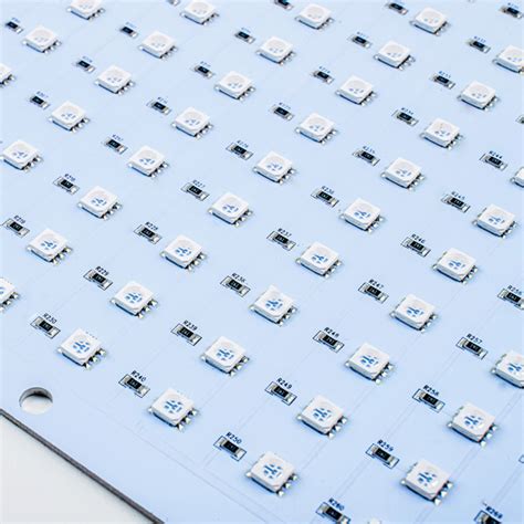
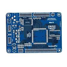
One of the primary techniques used in PCB assembly is Surface Mount Technology (SMT). SMT involves mounting electronic components directly onto the surface of the PCB.
This method is favored for its ability to accommodate a high density of components, making it ideal for modern, compact electronic devices. The process begins with the application of solder paste to the PCB using a stencil. Components are then placed onto the board using automated machines known as pick-and-place machines. These machines are highly accurate and can place thousands of components per hour. Once the components are in place, the board is passed through a reflow oven, where the solder paste melts and solidifies, creating strong electrical connections.
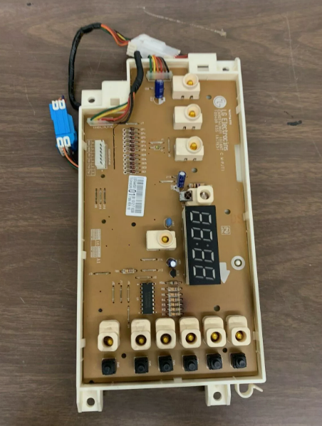
In contrast to SMT, Through-Hole Technology (THT) involves inserting component leads through pre-drilled holes in the PCB.
This technique is often used for components that require a stronger mechanical bond, such as connectors or large capacitors. The process starts with the manual or automated insertion of component leads into the holes. The board is then subjected to a wave soldering process, where it passes over a wave of molten solder. The solder adheres to the exposed metal surfaces, forming secure connections. While THT is less common in modern electronics due to its space requirements, it remains valuable for specific applications.
Another important technique in PCB assembly is the use of Automated Optical Inspection (AOI).
AOI systems employ cameras and sophisticated software to inspect PCBs for defects such as misaligned components, solder bridges, or missing parts. This non-contact method allows for rapid and accurate inspection, ensuring that any issues are identified and corrected early in the production process. AOI is particularly useful in high-volume manufacturing, where manual inspection would be impractical.
In addition to AOI, X-ray inspection is another technique used to ensure the quality of PCB assemblies. X-ray inspection is particularly effective for detecting hidden defects, such as voids in solder joints or internal cracks in components. This method provides a detailed view of the internal structure of the PCB, allowing for thorough quality control. While more expensive than AOI, X-ray inspection is invaluable for critical applications where reliability is paramount.
Furthermore, functional testing is a crucial step in PCB assembly.
This involves subjecting the assembled PCB to a series of tests to verify that it operates as intended. Functional testing can range from simple continuity checks to complex simulations of the PCB’s operating environment. This step ensures that any functional defects are identified and rectified before the PCB is integrated into the final product.
In conclusion, PCB assembly relies on a combination of techniques to achieve high-quality, reliable electronic circuits. Surface Mount Technology and Through-Hole Technology provide the means to mount components, while Automated Optical Inspection and X-ray inspection ensure the integrity of the assembly. Functional testing further guarantees that the PCB performs as expected. By employing these techniques, manufacturers can produce sophisticated electronic devices that meet the demands of today’s technology-driven world.
Quality Control Measures In PCB Assembly
Quality control measures in PCB assembly are critical to ensuring the reliability and functionality of the final product. The process begins with the inspection of raw materials, where components and substrates are scrutinized for any defects or inconsistencies. This initial step is crucial because any flaw in the raw materials can compromise the entire assembly process. Once the materials pass this initial inspection, the assembly process can commence.
During the assembly process, several automated and manual inspections are conducted to maintain high standards.
Automated Optical Inspection (AOI) is one of the primary methods used. AOI systems utilize high-resolution cameras to capture images of the PCB and compare them against a predefined standard. This method is highly effective in identifying issues such as soldering defects, component misalignment, and missing components. By catching these issues early, AOI helps to minimize the risk of defects in the final product.
In addition to AOI, X-ray inspection is employed to examine the internal structures of the PCB. This technique is particularly useful for detecting hidden defects such as voids in solder joints and misaligned layers. X-ray inspection provides a non-destructive means of ensuring the integrity of the assembly, which is essential for maintaining the reliability of the final product.
Manual inspections also play a vital role in quality control.
Skilled technicians perform visual inspections to identify any defects that automated systems might miss. These inspections are often conducted at various stages of the assembly process, providing multiple opportunities to catch and correct issues. The human element in quality control adds an additional layer of scrutiny, ensuring that even the smallest defects are identified and addressed.
Functional testing is another critical component of quality control in PCB assembly. This involves subjecting the assembled PCB to a series of tests to verify its performance under various conditions. Functional testing can include electrical tests, thermal cycling, and environmental stress tests. These tests are designed to simulate real-world conditions and ensure that the PCB will perform reliably in its intended application. By rigorously testing the PCB, manufacturers can identify and rectify any issues before the product reaches the customer.
Furthermore, statistical process control (SPC) is employed to monitor and control the assembly process.
SPC involves collecting data at various stages of the assembly process and using statistical methods to identify trends and variations. By analyzing this data, manufacturers can identify potential issues and implement corrective actions before they result in defects. SPC helps to maintain consistent quality and reduce the likelihood of defects in the final product.
Finally, traceability is an essential aspect of quality control in PCB assembly.
Traceability involves maintaining detailed records of each step in the assembly process, including the origin of raw materials, the specific processes used, and the results of inspections and tests. This information is invaluable in the event of a defect, as it allows manufacturers to trace the issue back to its source and implement corrective actions. Traceability also provides a means of verifying that all quality control measures have been followed, ensuring that the final product meets the highest standards of quality.
In conclusion, quality control measures in PCB assembly are multifaceted and involve a combination of automated and manual inspections, functional testing, statistical process control, and traceability. Each of these measures plays a critical role in ensuring the reliability and functionality of the final product. By rigorously implementing these quality control measures, manufacturers can minimize the risk of defects and deliver high-quality PCBs that meet the stringent demands of their customers.