How does PCB reflow occur? The role of PCB reflow line
1. Basic concept of reflow
In the schematic diagram of digital circuit, the propagation of digital signal is from one logic gate to another. The signal is sent from the output end to the receiving end through the wire. It seems to flow in one direction. Many digital engineers therefore think that the loop path is irrelevant. After all, both the driver and the receiver are specified as voltage mode devices. Why should we consider the current?
In fact, basic circuit theory tells us that the signal is propagated by the current, that is, the movement of electrons. One of the characteristics of electron flow is that electrons never stay anywhere. No matter where the current flows, it must come back. Therefore, the current always flows in the loop, and any signal in the circuit exists in the form of a closed loop.
For high-frequency signal transmission, it is actually the process of charging the dielectric capacitor sandwiched between the transmission line and the DC layer.
2. The impact of reflow
Digital circuits usually use ground and power planes to complete reflow. The reflow paths of high-frequency signals and low-frequency signals are different. The reflow of low-frequency signals chooses the impedance path, and the reflow of high-frequency signals chooses the inductive reactance path.
When the current starts from the signal driver, flows through the signal line, and is injected into the receiving end of the signal, there is always a return current in the opposite direction: starting from the ground pin of the load, passing through the copper plane, and flowing to the signal source, forming a closed loop with the current flowing through the signal line.
The noise frequency caused by this current flowing through the copper plane is equivalent to the signal frequency. The higher the signal frequency, the higher the noise frequency. The logic gate does not respond to the input signal, but to the difference between the input signal and the reference pin.
The circuit with a single point termination responds to the difference between the incoming signal and its logic ground reference plane, so the disturbance on the ground reference plane and the interference on the signal path are equally important.
The logic gate responds to the input pin and the specified reference pin. We don’t know which is the specified reference pin (for TTL, it is usually the negative power supply, and for ECL, it is usually the positive power supply, but not all of them are like this). In terms of this property, the anti-interference ability of the differential signal can have a good effect on ground bounce noise and power plane sliding.
When many digital signals on the PCB are switched synchronously (such as the data bus and address bus of the CPU), this causes transient load current to flow from the power supply into the circuit or from the circuit into the ground line. Due to the impedance of the power line and the ground line, synchronous switching noise (SSN) will be generated, and ground plane bounce noise (referred to as ground bounce) will also appear on the ground line.
When the surrounding area of the power line and the ground line on the printed circuit board is larger, their radiation energy will be greater. Therefore, we analyze the switching state of the digital chip and take measures to control the return flow mode to achieve the purpose of reducing the surrounding area and radiation degree.
Example explanation:
IC1 is the signal output terminal, IC2 is the signal input terminal (to simplify the PCB model, it is assumed that the receiving end contains a bottom connection resistor), and the third layer is the ground layer. The ground of IC1 and IC2 comes from the third layer of the ground layer.
The upper right corner of the TOP layer is a power plane, which is connected to the positive pole of the power supply. C1 and C2 are the decoupling capacitors of IC1 and IC2 respectively. The power supply and ground pins of the chip shown in the figure are both the power supply and ground of the transmitting and receiving signal ends.
At low frequency, if the S1 end outputs a high level, the entire current loop is that the power supply is connected to the VCC power plane through the wire, then enters IC1 through the orange path, then comes out from the S1 end, enters IC2 through the second layer of wires through the R1 end, then enters the GND layer, and returns to the negative pole of the power supply through the red path.
At high frequency, the distribution characteristics presented by the PCB will have a great impact on the signal. The ground return we often say is a problem that is often encountered in high-frequency signals.
When there is an increased current in the signal line from S1 to R1, the external magnetic field changes rapidly, which will cause the nearby conductor to induce a reverse current. If the ground plane of the third layer is a complete ground plane, then a current marked by a blue dotted line will be generated on the ground plane. If the TOP layer has a complete power plane, there will also be a return along the blue dotted line on the TOP layer.
At this time, the signal loop has a current loop, the energy radiated outward, and the ability to couple external signals is also. (The skin effect at high frequencies also radiates energy outwards, and the principle is the same.)
Since the high-frequency signal level and current change very quickly, but the change cycle is short, the energy required is not very large, so the chip is powered by the decoupling capacitor close to the chip.
When C1 is large enough and reacts quickly enough (with a very low ESR value, ceramic capacitors are usually used. The ESR of ceramic capacitors is much lower than that of tantalum capacitors.), the orange path on the top layer and the red path on the GND layer can be regarded as non-existent (there is a current corresponding to the power supply of the entire board, but not the current corresponding to the signal in the figure).
Therefore, according to the environment constructed in the figure, the entire path of the current is: from the positive pole of C1 → VCC of IC1 → S1 → L2 signal line → R1 → GND of IC2 → via → yellow path of the GND layer → via → negative pole of the capacitor.
It can be seen that there is a brown equivalent current in the vertical direction of the current, and a magnetic field will be induced in the middle. At the same time, this ring surface can also be easily coupled to external interference. If the signal in the figure is a clock signal, and there is a group of 8-bit data lines in parallel, powered by the same power supply of the same chip, the current return path is the same.
If the data line level flips in the same direction at the same time, a large reverse current will be induced on the clock. If the clock line is not well matched, this crosstalk is enough to have a fatal impact on the clock signal.
The intensity of this crosstalk is not proportional to the high and low levels of the interference source, but proportional to the current change rate of the interference source. For a purely resistive load, the crosstalk current is proportional to:
dI/dt=dV /(T?10%-90%*R)
In the formula, dI/dt (current change rate), dV (swing amplitude of the interference source) and R (interference source load) all refer to the parameters of the interference source (if it is a capacitive load, dI/dt is inversely proportional to the square of T?10%-90%). It can be seen from the formula that low-frequency signals may not have less crosstalk than high-speed signals.
That is what we said: 1KHz signal is not necessarily a low-speed signal, and the edge situation should be considered comprehensively. For signals with very steep edges, they contain many harmonic components and have large amplitudes at each frequency doubling point.
Therefore, when selecting devices, you should also pay attention to not blindly choose chips with fast switching speeds. Not only is the cost high, but it will also increase crosstalk and EMC problems.
Any adjacent power layer or other plane, as long as there is a suitable capacitor at both ends of the signal to provide a low-reactance path to GND, then this plane can be used as the return plane of this signal.
In ordinary applications, the IO power supply of the chip corresponding to the transmitter and receiver is often consistent, and there are generally 0.01-0.1uF decoupling capacitors between their respective power supplies and ground, and these capacitors are just at both ends of the signal, so the return effect of the power plane is second only to the ground plane.
If other power planes are used for return, there will often be no low-reactance path to the ground at both ends of the signal. In this way, the current induced in the adjacent plane will find the nearest capacitor to return to the ground.
If this “close capacitor” is far away from the beginning or the end, the return current will also have to “travel a long way” to form a complete return path, and this path is also the return path of the adjacent signal. The effect of this same return path is the same as the common ground interference, which is equivalent to the crosstalk between signals.
For some unavoidable cross-power splitting situations, a high-pass filter composed of a capacitor or RC series connection can be connected across the splitting place (such as a 10 ohm resistor in series with a 680p capacitor. The specific value depends on the type of signal, that is, to provide a high-frequency return path and isolate the low-frequency crosstalk between the planes).
This may involve the problem of adding capacitors between power planes, which seems a bit funny, but it is definitely effective. If some specifications do not allow it, the capacitors can be connected to the ground at the splitting point.
For the situation of borrowing other planes for return, a few small capacitors can be appropriately added to the ground at both ends of the signal to provide a return path. But this approach is often difficult to achieve. Because most of the surface space near the terminal is occupied by matching resistors and chip decoupling capacitors.
Backflow noise is one of the main noises on the reference plane. Therefore, it is necessary to study the path and flow range of the return current.
3.Theoretical knowledge of return path
The figure below shows a line in the printed circuit board. There is current passing through the wire. Usually, we only see the wires laid on the surface for transmitting signals, from the driving end to the receiving end. In fact, the current can only flow in the loop. The transmission line is visible to us, and the path of the current return is usually invisible. They usually flow back with the help of the ground plane and the power plane. Since there is no physical line, the loop path becomes difficult to estimate, and it is difficult to control them.
As shown in Figure 3.1, each wire and its loop on the PCB board constitute a current loop. According to the principle of electromagnetic radiation, when the sudden current flows through the wire loop in the circuit, an electromagnetic field will be generated in space and affect other wires. This is what we usually call radiation. In order to reduce the impact of radiation, we should first understand the basic principles of radiation and parameters related to radiation intensity.
Figure 3.1 Differential mode radiation on a printed circuit board
These loops are equivalent to small antennas that are working, radiating magnetic fields into space. We simulate it with the radiation generated by a small loop antenna. Assume that the current is I and the area is S. The electric field strength measured in the far field of free space r is:
E–Electric field
f–Frequency
S–Area
I–Current
r–Distance
Equation 3.1 is applicable to small loops placed in free space with no surface reflection. In fact, our products are on the ground instead of free space. The reflection of the nearby ground will increase the measured radiation by 6dB. Considering this, equation 3.1 must be multiplied by 2. If the ground reflection is corrected and assumed to be the radiation direction, equation 3.1 is From equation 3.2, we know that the radiation is proportional to the loop current and the loop area, and proportional to the square of the current frequency.
The path of the return current in a printed circuit board is closely related to the frequency of the current. According to basic circuit knowledge, direct current or low-frequency current always flows in the direction of impedance; while high-frequency current always flows in the direction of inductive reactance when resistance is constant.
If the influence of holes and grooves formed by vias on the copper plane is not considered, the impedance path, that is, the path of low-frequency current, is composed of arc lines on the ground copper plane, as shown in Figure 3.2. The density of current on each arc line is related to the resistivity on this arc line.
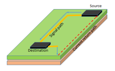
Figure 3.2 High-frequency current path on PCB copper plane
For transmission lines, the return path of inductive reactance, that is, the return path of high-frequency current, is on the copper plane directly below the signal wiring, as shown in Figure 3.3. Such a return path makes the space area surrounded by the entire loop, which also makes the magnetic field strength (or the ability to receive space radiation) of the loop antenna formed by this signal radiate to space.
For relatively long and straight wiring, it can be regarded as an ideal transmission line. The signal return current propagating on it flows through a strip area with the signal wiring as the central axis. The farther away from the center axis of the signal wiring, the smaller the current density,
As shown in Figure 3.3. This relationship approximately satisfies Formula 3.3 [4]:
Formula 3.3
Where, is the original signal current, in units of “A, ampere”;
is the distance between the signal wiring and the copper plane, in units of “in., inch”;
is the vertical distance from a point on the copper plane to the signal line, in units of “in., inch”;
is the current density at this point, in units of “A/in., ampere per inch”. 2.1 Device selection
Figure 3.3 Transmission line return current density distribution diagram
According to Formula 3.3, Table 3.1 lists the percentage of the return current flowing through the strip area with a width of centered on the transmission line as a percentage of all return currents.
Assuming that the current returned through the area 0.035 inches away from the transmission line only accounts for 13% of all return currents, and only 6.5% is specifically distributed to one side of the transmission line, and the density is very small. Therefore, it can be ignored.
Summary:
- When there is a continuous, dense, and complete copper plane under the signal wiring, the noise interference of the signal return current on the copper plane is local.
Therefore, as long as the principle of layout and wiring localization is followed, that is, the distance between digital signal lines, digital devices and analog signal lines and analog devices is artificially pulled to a certain extent, the interference of digital signal return current on analog circuits can be greatly reduced.
- High-frequency transient return current flows back to the driver end through the plane (ground plane or power plane) adjacent to the signal routing.
The terminal load of the driver signal routing is connected across the signal routing and the plane (ground plane or power plane) adjacent to the signal routing.
- When the surrounding area of the power line and ground line on the printed circuit board is larger, their radiation energy is also greater.
Therefore, by controlling the return path, we can make the surrounding area smaller, thereby controlling the radiation level.
4.Solutions to the return problem
There are usually three aspects that cause return problems on PCB boards: chip interconnection, copper surface cutting, and via jumping. These factors are analyzed in detail below.
4.1 Return problems caused by chip interconnection
When a digital circuit is working, a conversion between high and low voltages will occur, which causes transient load current to flow from the power supply to the circuit or from the circuit to the ground.
For digital devices, its pin input resistance can be considered infinite, equivalent to an open circuit (i.e., i=0 in the figure below). In fact, the loop current returns through the distributed capacitance and distributed inductance generated by the chip, power supply, and ground plane. The following analysis takes the collector output circuit as an internal circuit of the output signal as an example.
4.1.1 The driver changes from a low level to a high level.
When the output signal jumps from low level to high level, it is equivalent to the output pin outputting a current to the transmission line. Since the input resistance is infinite, we believe that for the chip, no current flows into the input leg, that is, . Then, this current must beIt must return to the power leg of the output chip.
① The signal trace is close to the power plane
The driver end charges the transmission line formed by the signal trace, the power plane and the terminal load. The current enters the device from the power pin of the driver and flows from the output end of the driver to the load end;
The high-frequency transient return current flows back to the output end of the driver on the power plane below the signal trace. The return current directly passes through the power plane and enters the driver from the power pin of the driver to form a current loop.
② The signal trace is close to the ground plane
The driver charges the transmission line formed by the signal trace, the power plane and the terminal load. The current enters the device from the power pin of the driver and flows from the output end of the driver to the load end.
The high-frequency transient return current flows back to the output end of the driver on the ground plane below the signal trace. The return current must use the coupling capacitor of the power plane and the ground plane at the output end of the driver to cross from the ground plane to the power plane, and then enter the driver from the power pin of the driver to form a current loop.
4.1.2 The driver end changes from high level to low level, which is equivalent to the output pin absorbing the current on the transmission line.
① The signal line is close to the power plane
The load discharges the transmission line formed by the signal line, the power plane and the output end of the driver. The current enters the device from the output pin of the driver, flows out from the ground pin of the driver, enters the ground plane, and passes through the power plane and ground plane coupling capacitor near the ground pin of the driver, crosses to the power plane, and returns to the load end.
The high-frequency transient return current flows back to the load end on the power plane below the signal line, forming a current loop.
② The signal line is close to the ground plane
The load discharges the transmission line formed by the signal line, the power plane and the output end of the driver. The current enters the device from the output pin of the driver, flows out from the ground pin of the driver, enters the ground plane, and returns to the load end; the high-frequency transient return current flows back to the load end on the ground plane below the signal line, forming a current loop.
Near the output pins and ground pins of the driver, the coupling capacitors of the power plane and the ground plane should be placed to provide a return path for the return current. Otherwise, the return current will seek the coupling path of the power plane and the ground plane to return (making the return path difficult to predict and control, thus causing crosstalk to other traces).
4.2 Solution to the return problem caused by copper cladding cutting
The ground plane and the power plane can reduce the voltage loss caused by resistance.
As shown in the figure, the loop current flows back through the ground. Due to the existence of resistor R1, a voltage drop is bound to occur at points 1 and 2. The larger the resistance, the greater the voltage drop, causing inconsistency with the ground level. If there is a ground layer, it can be regarded as a signal line with infinite line width and very small resistance.
The loop current always flows through the ground layer close to the signal. When there is more than one layer, if the signal is between two layers of ground planes and the two are exactly the same, the loop current will be equally divided and pass through the two planes.
4.2.1 Under the condition of localized layout and wiring:
The digital ground plane and the analog ground plane share the same copper plane, that is, there is no distinction between digital ground and analog ground, and the noise of the digital circuit itself does not bring additional noise to the analog circuit system.
4.2.2 In the digital and analog mixed circuit system:
The common point of the digital ground and the analog ground is selected outside the board, that is, the two copper planes are completely independent, so that the signal line between the digital circuit and the analog circuit does not have the characteristics of a transmission line, which brings serious signal integrity problems to the system.
The digital circuit and the analog circuit use the same power supply system, and the ground plane is not divided. In the design of the digital and analog mixed circuit system, on the basis of modular layout and localized wiring, the digital circuit module and the analog circuit module share a complete, undivided voltage reference plane, which will not only not increase the interference of the digital circuit to the analog circuit, but also greatly reduce the crosstalk between signals and the ground bounce noise of the system due to the elimination of the “cross-trench” problem of the signal line, and improve the front-end analog circuit.
4.3 Solution to the backflow problem caused by vias
When routing signals on a printed circuit board, if it is a multi-layer board, many signals must complete the connection task by changing layers, and a large number of vias are needed at this time.
There are two effects of vias on backflow: one is that the vias form grooves to block the backflow, and the other is that the backflow jumps layer caused by the vias.
4.3.1 Grooves formed by vias
When routing signals on a printed circuit board, if it is a multi-layer board, many signals must complete the connection task by changing layers, and a large number of vias are needed at this time. If the vias are arranged densely on the power or ground plane, sometimes many vias will be connected together to form the so-called groove, as shown in the figure.
First, we should analyze this situation to see if the backflow needs to pass through the groove. If the backflow of the signal does not need to pass through the groove, it will not hinder the backflow.
If the loop circuit has to bypass this groove to return, the antenna effect formed will increase sharply, causing interference to the surrounding signals. Usually, after the coating data is generated, we can adjust the places where the vias are too dense and form grooves, so that there is a certain distance between the vias.
4.3.2 Layer jump phenomenon formed by vias
Let’s take a six-layer board as an example for analysis. The six-layer board has two coating layers, the second layer is the ground layer, and the fifth layer is the power layer.
Therefore, the signal return of the surface layer and the third layer is mainly in the ground layer; the return of the bottom layer and the fourth layer is mainly in the power layer. There are six possibilities when changing layers: surface layer <—–> third layer, surface layer <—–> fourth layer, surface layer <—–> bottom layer, third layer <—–> fourth layer, third layer <—–> bottom layer, fourth layer <—–> bottom layer.
These six possible situations can be divided into two categories according to the situation of the loop current: the situation where the loop current flows on the same layer and on different layers, that is, whether there is a layer jump phenomenon.
A. The situation where the loop current flows on the same layer includes the surface layer <—–> third layer and the fourth layer <—–> bottom layer, as shown in the figure.
In this case, the loop current flows on the same layer. However, according to the principle of electrostatic induction, the internal electric field strength of a complete conductor in an electric field is zero, and all currents flow on the surface of the conductor. The ground plane and the power plane are actually such a conductor.
The vias we use are all through holes. The holes left by these vias passing through the power and ground planes provide a path for the current to flow through the upper and lower surfaces of the coating layer. Therefore, the return path of these signal lines is very good and no measures are needed to improve it.
B. The situation where the loop current flows on different layers includes the surface layer <—–> the fourth layer, the surface layer <—–> the bottom layer, the third layer <—–> the fourth layer, and the third layer <—–> the bottom layer. The following takes the surface layer <—–> the bottom layer and the third layer <—–> the fourth layer as examples to analyze the return flow.
For signals with layer skipping phenomenon, it is necessary to add some bypass capacitors near the dense area of vias, usually 0.1uf magnetic sheet capacitors, to provide a return path.