How important is PCB routing in PCB design?
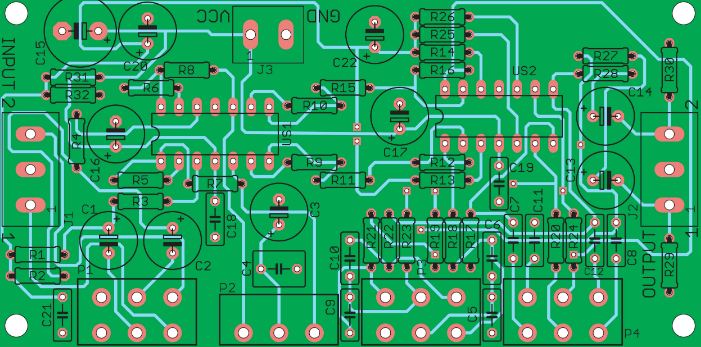
In PCB design, routing is a crucial step in completing a product design. It’s a process that demands the most skill and effort, requiring the most design expertise. PCB routing can be performed in single-sided, double-sided, or multi-layer modes. There are two routing methods:
Automatic routing and interactive routing. Before automatic routing, interactive routing can be used to pre-route lines with more stringent requirements. Avoid parallel paths between input and output edges to prevent reflection interference. Ground isolation should be added when necessary. Lines on adjacent layers should be perpendicular to each other; parallel paths can easily cause parasitic coupling.
The routing success rate of automatic routing depends on a good layout. Routing rules can be pre-set, including the number of bends, number of vias, and number of stepovers. Exploratory routing is generally performed first to quickly connect short lines. Then, maze routing is performed to optimize the routing paths of the lines to be routed. Routing can also be performed as needed to disconnect already routed lines and attempt to reroute them to improve the overall result.
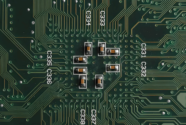
Through-hole vias are no longer suitable for today’s high-density PCB designs, wasting valuable routing channels. To address this issue, blind and buried via technologies have emerged. They not only fulfill the function of through-holes but also save numerous routing channels, making the routing process more convenient, smoother, and more complete. The PCB design process is both complex and simple. To fully master it, electronic engineers must gain personal experience and truly grasp its essence.

1.Power and Ground Wire Management
Even if the entire PCB layout is perfectly executed, interference caused by inconsiderate power and ground routing can degrade product performance and sometimes even impact product success rates. Therefore, careful attention must be paid to routing power and ground lines, minimizing the noise interference generated by these lines to ensure product quality. Every electronic product designer understands the causes of noise between ground and power lines. Here, we will discuss methods for reducing this noise:
It is well known that decoupling capacitors are added between the power and ground lines. Try to widen the power and ground traces as much as possible. Ideally, the ground trace should be wider than the power trace. The relationship between them is: ground > power > signal. Typical signal trace widths are 0.2-0.3mm, with the thinnest width reaching 0.05-0.07mm. Power traces are 1.2-2.5mm. For digital circuit PCBs, wide ground conductors can be used to form a loop, creating a ground grid (this is not recommended for analog circuit ground). Use a large copper layer as the ground trace, connecting unused areas on the printed circuit board to the ground. Alternatively, create a multilayer board, with the power and ground traces each occupying one layer.
2.Common Grounding for Digital and Analog Circuits
Many PCBs now no longer consist of single-function circuits (digital or analog), but instead contain a mix of digital and analog circuits.
Therefore, when routing, it’s important to consider interference between these circuits, especially noise interference on the ground traces. Digital circuits have high frequencies, and analog circuits are highly sensitive. High-frequency signal lines should be kept as far away from sensitive analog circuit components as possible. For ground lines, the entire PCB has only one connection to the outside world, so common grounding for both digital and analog circuits must be addressed internally. Internally, the digital and analog grounds are actually separate and unconnected, connecting only at interfaces (such as connectors) where the PCB connects to the outside world. Note that there is a single connection point between the digital and analog grounds. Sometimes, these grounds are not shared on the PCB; this depends on the system design.
3.Routing Signal Lines on the Power (Ground) Layer
When routing multilayer PCBs, there are only a few unfinished signal layers. Adding additional layers would be wasteful, increase production workload, and increase costs. To address this conflict, routing on the power (ground) layer can be considered. The power layer should be used first, followed by the ground layer, as it is best to preserve the integrity of the ground layer.

4.Treatment of Connector Legs in Large-Area Conductors
In large-area grounding (electrical) systems, component legs are often connected to them. The treatment of these legs requires comprehensive consideration. From an electrical performance perspective, full contact between the component leg pads and the copper surface is optimal. However, this poses several risks to component soldering and assembly, such as:
① Soldering requires a high-power heater. ② It can easily cause cold solder joints.
To balance electrical performance and process requirements, a cross-shaped solder pad, known as a heat shield, is used.
This greatly reduces the likelihood of cold solder joints caused by excessive heat dissipation across the cross section during soldering. The treatment of the electrical (ground) legs of multilayer boards is similar.
5.The Role of Network Systems in Wiring
In many CAD systems, wiring is determined by the network system. An overly dense grid increases the number of paths, but the step size is too small, resulting in excessive drawing data. This inevitably increases the storage space required for the device and significantly impacts the computing speed of computer electronics. However, some paths are ineffective, such as those occupied by component leg pads, mounting holes, or fixed holes. An overly coarse grid with too few paths significantly impacts routing efficiency. Therefore, a well-balanced grid system is essential to support routing.
The distance between standard component legs is 0.1 inch (2.54 mm), so the basis of the grid system is generally set at 0.1 inch (2.54 mm) or an integer multiple of 0.1 inch, such as 0.05 inch, 0.025 inch, or 0.02 inch.
6.Design Rule Check (DRC)
After completing the routing design, it is necessary to carefully check whether the routing design complies with the rules established by the designer. It is also necessary to confirm whether the established rules meet the requirements of the printed circuit board production process. This check generally includes the following aspects:
A. Whether the distances between lines, lines and component pads, lines and through-holes, component pads and through-holes, and through-holes are reasonable and meet production requirements.
B. Are the widths of the power and ground traces appropriate? Are they tightly coupled (low impedance)? Are there areas on the PCB where the ground traces can be widened?
C. Have optimal measures been taken for critical signal traces, such as minimizing length, adding guard lines, and clearly separating input and output lines?
D. Do analog and digital circuits have separate ground traces?
E. Will graphics added to the PCB later (such as icons and annotations) cause signal short circuits?
F. Modify any undesirable line shapes.
G. Are process lines added to the PCB? Does the solder mask meet production process requirements? Is the solder mask size appropriate?
Does the logo mark press against the device pads to avoid compromising the quality of the electrical assembly?
H. Is the outer edge of the power and ground layer in a multilayer board narrowed? If the copper foil of the power and ground layer is exposed outside the board, it can easily cause short circuits.


