How Many Layers Should a Standard PCB Have?
Printed Circuit Boards (PCBs) are the backbone of modern electronics, providing mechanical support and electrical connections for components. One of the most critical design decisions is determining the number of layers a PCB should have. The optimal layer count depends on factors such as circuit complexity, signal integrity, power requirements, cost, and manufacturing constraints.
This article explores the typical layer configurations for standard PCBs, their advantages and disadvantages, and guidelines for selecting the right number of layers for different applications.
1. Understanding PCB Layers
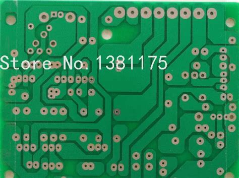
A PCB consists of conductive copper layers laminated between insulating dielectric materials (typically FR4). The layers are interconnected using vias (plated holes) to form a complete circuit. PCBs can be categorized into three main types based on layer count:
- Single-layer PCBs (1-layer)
- Double-layer PCBs (2-layer)
- Multi-layer PCBs (4, 6, 8, or more layers)
Each configuration serves different purposes depending on the design requirements.
2. Single-Layer PCBs (1-Layer)
Structure:
- One conductive copper layer on a substrate.
- Components are placed on one side, and traces are routed on the other.
Advantages:
✅ Lowest cost – Minimal material and manufacturing complexity.
✅ Simple fabrication – Easy to design and produce.
✅ Suitable for low-frequency circuits – Ideal for basic electronics like LED boards, simple sensors, and power supplies.
Disadvantages:
❌ Limited routing space – Complex circuits may require jumpers or manual wiring.
❌ Poor signal integrity – Not suitable for high-speed or noise-sensitive designs.
❌ No ground/power planes – Increased EMI susceptibility.
Typical Applications:
- Consumer electronics (toys, calculators).
- Simple power supplies.
- Basic hobbyist projects.
3. Double-Layer PCBs (2-Layer)
Structure:
- Two conductive layers (top and bottom) with through-hole vias connecting them.
Advantages:
✅ Better routing flexibility – More space for traces than single-layer PCBs.
✅ Improved signal integrity – Ground fills can reduce noise.
✅ Moderate cost – Still affordable for many applications.
Disadvantages:
❌ Still limited for complex designs – High-density circuits may require more layers.
❌ Signal crosstalk issues – Without proper shielding, high-speed signals may interfere.
Typical Applications:
- Arduino and Raspberry Pi shields.
- Motor controllers.
- Intermediate hobbyist and prototyping projects.
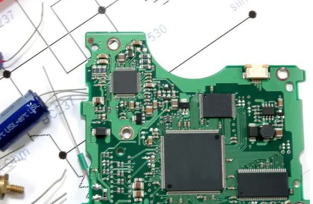
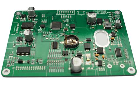
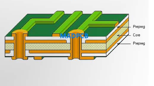
4. Multi-Layer PCBs (4+ Layers)
Multi-layer PCBs stack multiple conductive layers (typically in even numbers) to improve performance. Common configurations include 4-layer, 6-layer, 8-layer, and beyond.
4-Layer PCBs
Structure:
- Top Layer (Signal)
- Inner Layer 1 (Ground Plane)
- Inner Layer 2 (Power Plane)
- Bottom Layer (Signal)
Advantages:
✅ Improved EMI shielding – Dedicated ground and power planes reduce noise.
✅ Better signal integrity – Controlled impedance for high-speed signals.
✅ Higher component density – More routing options without jumpers.
Disadvantages:
❌ Higher cost than 2-layer PCBs – Additional materials and lamination steps.
Typical Applications:
- Embedded systems (IoT devices).
- USB, HDMI, and Ethernet interfaces.
- Industrial control systems.
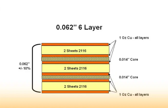
6-Layer PCBs
Structure:
- Top Layer (Signal)
- Inner Layer 1 (Ground)
- Inner Layer 2 (Signal)
- Inner Layer 3 (Power)
- Inner Layer 4 (Signal)
- Bottom Layer (Ground)
Advantages:
✅ Enhanced signal routing – More layers allow for better high-speed design.
✅ Reduced crosstalk – Shielding between signal layers.
Disadvantages:
❌ Higher fabrication cost – More complex manufacturing.
Typical Applications:
- High-speed digital circuits (DDR memory, FPGAs).
- RF and wireless communication devices.
8-Layer and Beyond
Structure:
- Typically includes multiple ground/power planes and signal layers.
- Used for extremely complex designs (e.g., processors, server motherboards).
Advantages:
✅ Optimal for high-speed, high-density designs – Supports GHz+ signals.
✅ Excellent power distribution – Multiple power planes reduce voltage drops.
Disadvantages:
❌ Expensive and complex to manufacture – Requires advanced PCB fabrication techniques.
Typical Applications:
- Smartphones and tablets.
- Advanced computing (CPUs, GPUs).
- Aerospace and military electronics.
5. How to Choose the Right Number of Layers
Key Considerations:
- Circuit Complexity
- Simple circuits: 1 or 2 layers.
- Moderate complexity: 4 layers.
- High-speed digital/RF: 6+ layers.
- Signal Integrity Requirements
- High-frequency signals need ground planes (4+ layers).
- Power Distribution
- Multiple voltage rails may require additional power planes.
- Cost Constraints
- More layers = higher manufacturing cost.
- Manufacturing Capabilities
- Not all PCB manufacturers support high-layer counts.
General Guidelines:
| Application | Recommended Layers |
|---|---|
| Simple circuits (LEDs, sensors) | 1-2 |
| Hobbyist projects (Arduino shields) | 2 |
| Consumer electronics (IoT, USB devices) | 4 |
| High-speed digital (DDR, FPGAs) | 6-8 |
| Advanced computing (CPUs, GPUs) | 8+ |
6. Conclusion
The number of layers in a standard PCB depends on the application’s complexity, performance needs, and budget. While single and double-layer PCBs are cost-effective for simple designs, 4 to 6-layer PCBs are ideal for most industrial and consumer electronics. 8-layer and beyond are reserved for high-performance computing and RF applications.
By carefully evaluating signal integrity, power requirements, and cost, engineers can select the optimal layer count for their PCB design, ensuring reliability and performance without unnecessary expenses.