How Signals Are Transmitted on a PCB: A Comprehensive Guide
Introduction
Printed Circuit Boards (PCBs) form the backbone of modern electronics, providing the physical platform for electrical components and the pathways for signal transmission between them. Understanding how signals propagate across PCBs is fundamental for electronics design, troubleshooting, and optimization. This 2000-word article explores the mechanisms, challenges, and design considerations involved in PCB signal transmission.
The Fundamentals of PCB Signal Transmission
1. Basic PCB Structure
A typical PCB consists of multiple layers of conductive copper traces separated by insulating dielectric material. These layers include:
- Signal layers: Where most component interconnections are routed
- Power planes: Provide stable voltage distribution
- Ground planes: Serve as reference points and return paths
- Dielectric material: Typically FR-4, which separates conductive layers
2. Signal Propagation Mechanism
Electrical signals travel through PCB traces as electromagnetic waves, not simply as electron flow. This propagation occurs through the interaction between:
- Electric fields between the signal trace and reference plane
- Magnetic fields surrounding the trace
The signal’s energy is contained within this electromagnetic field, which moves at a significant fraction of the speed of light (typically 50-70% depending on the dielectric material).
Types of Signal Transmission on PCBs
1. Single-ended Signaling
The most common transmission method where:
- A single trace carries the signal
- The return current flows through a ground plane or adjacent ground trace
- Simple to implement but susceptible to noise and interference
2. Differential Signaling
Used for high-speed or noise-sensitive applications:
- Two traces carry equal but opposite signals
- The receiver detects the voltage difference between them
- Benefits include:
- High noise immunity (common-mode rejection)
- Reduced electromagnetic interference (EMI)
- Better signal integrity at high frequencies
3. Transmission Line Techniques
At high frequencies (typically above 50-100MHz), PCB traces behave as transmission lines requiring special consideration:
- Controlled impedance becomes critical
- Proper termination is necessary to prevent reflections
- Common transmission line types on PCBs:
- Microstrip (trace on outer layer over ground plane)
- Stripline (trace embedded between two ground planes)
Critical Factors Affecting Signal Transmission
1. Impedance and Its Control
Characteristic impedance (typically 50Ω or 100Ω for differential pairs) depends on:
- Trace width and thickness
- Dielectric material properties (εᵣ)
- Distance to reference plane
- Consistent impedance prevents signal reflections and maintains integrity
2. Signal Integrity Challenges
Several phenomena can degrade signal quality:
a. Reflections:
- Occur at impedance discontinuities (vias, connectors, trace width changes)
- Can cause ringing and signal distortion
- Mitigated by proper termination and impedance control
b. Crosstalk:
- Unwanted coupling between adjacent traces
- Includes:
- Capacitive coupling (electric fields)
- Inductive coupling (magnetic fields)
- Reduced by:
- Adequate spacing between traces
- Guard traces or ground shielding
- Orthogonal routing of sensitive traces
c. Attenuation:
- Signal loss due to:
- Conductor resistance (more significant at high frequencies due to skin effect)
- Dielectric absorption
- Becomes critical for high-speed/long-distance traces
3. Return Current Path Considerations
Current always forms a complete loop, and the return path is as important as the signal trace:
- At low frequencies, return current takes the path of least resistance
- At high frequencies, return current follows the path of least inductance (directly beneath the signal trace)
- Interruptions in return paths (splits in ground planes) can cause serious signal integrity issues
High-Speed Design Considerations
1. Signal Rise Time vs. Trace Length
When trace length approaches a significant fraction of the signal’s wavelength (typically 1/10th), transmission line effects become important:
- Critical length ≈ (rise time × propagation velocity)/6
- For fast rise times (<1ns), even short traces may require transmission line treatment
2. Propagation Delay and Timing
Signal propagation speed in PCB traces:
- v = c/√εᵣ
- c = speed of light in vacuum
- εᵣ = dielectric constant (≈4.3 for FR-4)
- Results in ≈140-180ps/inch delay (depending on εᵣ)
- Critical for synchronous systems and matched-length requirements
3. Power Integrity Considerations
Signal transmission is closely tied to power distribution:
- Simultaneous switching noise can couple into signals
- Proper decoupling capacitor placement is essential
- Power plane resonance can affect signal quality
PCB Materials and Their Impact
1. Dielectric Materials
Common materials and their properties:
- FR-4: Standard material, εᵣ≈4.3, lossy at high frequencies
- High-frequency laminates (Rogers, Isola): Lower εᵣ and loss tangent for RF/microwave
- Flex materials: Polyimide for flexible circuits
2. Copper Properties
- Standard 1oz (35μm) and 2oz (70μm) copper weights
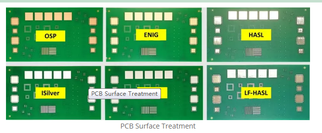
- Surface roughness affects high-frequency losses
- Plating options (ENIG, immersion silver, OSP) impact signal quality
Design Techniques for Optimal Signal Transmission
1. Routing Best Practices
- Maintain consistent trace widths for impedance control
- Minimize sharp bends (use 45° or curved traces)
- Avoid stubs in high-speed lines
- Provide adequate clearance to other traces/features
2. Via Management
Vias create impedance discontinuities and can:
- Introduce inductance (problematic for high-speed returns)
- Cause reflections
- Strategies:
- Use appropriate via sizes
- Provide return vias adjacent to signal vias
- Consider back-drilling for critical RF signals
3. Grounding Techniques
- Use solid ground planes when possible
- Implement proper stitching via placement
- Separate analog and digital grounds appropriately
- Consider split planes only when necessary
Simulation and Verification
Modern PCB design relies heavily on simulation tools:
- Signal integrity analysis: Predict reflections, crosstalk
- EM simulation: Analyze electromagnetic field behavior
- Power integrity analysis: Verify power delivery network
- 3D EM solvers: For complex structures and connectors
Measurement techniques:
- Time Domain Reflectometry (TDR) for impedance verification
- Vector Network Analysis (VNA) for frequency response
- Eye diagram analysis for high-speed serial links

Emerging Technologies and Future Trends
1. Higher Frequency Challenges
As signals approach mmWave frequencies (30GHz+):
- Material properties become more critical
- Surface roughness effects are more pronounced
- 3D integration and advanced packaging gain importance
2. Advanced Materials
- Low-loss dielectrics for 5G and automotive radar
- Embedded passive components
- Carbon nanotube and graphene interconnects (research stage)
3. Photonic Integration
- Optical interconnects on PCBs for extremely high bandwidth
- Hybrid electrical/optical circuit boards
Conclusion
Signal transmission on PCBs is a complex interplay of electromagnetic theory, material science, and practical engineering constraints. As electronic systems continue to push toward higher speeds and greater complexity, understanding these fundamental principles becomes ever more critical. By carefully considering signal integrity, power integrity, and electromagnetic compatibility during the design phase, engineers can create PCBs that reliably transmit signals while meeting performance requirements. The field continues to evolve with new materials, design techniques, and simulation tools enabling ever more sophisticated electronic systems.