How Signals Propagate in PCBs
Designing printed circuit boards for electromagnetic compatibility(EMC) requires a deep understanding of signal propagation from the perspective of electromagnetic fields and currents.they help us design PCBs with low electromagnetic field emission and low sensitivity to external radiation or interference.
In the first article in the “Mastering EMI Control in PCB design”series, we will delve deeper into these concept and see how they apply to pcb design.
Concepts of signal Propagation in Transmission Lines
When thinking about how signals propagate in PCBs,it’s important to shift from the analogy of”water flowing through a pipe”to one based on electromagnetic fields and transmission lines.A transmission line is a structure designed to transfer energy from one point to another in the form of confined electromagnetic fields.In a PCB, a transmission line consist of at least two conductors-both of which are equally important in confining and directing electromagnetic fields from one point in the circuit to another.If one of these conductors is missing,the electromagnetic fields that make up the signal are not confined,and the spread of these fields can cause EMC testing failure.
This leads to a very important concept:electromagnetic signals are not contained within conductor,but rather exist in the dielectric between the two conductors and in the surrounding space.From an EMC perspective ,the goal is to maximize the confined electromagnetic field between the two conductors and minimize the electromagnetic field around them.
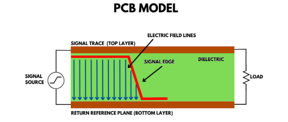
Figure 1: Schematic diagram of digital signal propagation in a PCB
In a PCB, the two conductors used for signal propagation are the signal potential conductor and the return and reference potential conductor. The most intuitive example is a two-layer board: the top layer connects to the signal source and is used to route signal traces; the bottom layer is a solid copper layer that connects both the signal source and the signal potential reference (see Figure 1). What we call a “signal” is actually the electromagnetic field between these two conductors—this means that the signal does not reside in a single conductor, but rather is electromagnetic energy in the dielectric between the two conductors. This also shows that the properties of the dielectric material affect signal propagation, particularly the speed of signal (or electromagnetic wave) propagation, which is equivalent to the speed of light in the dielectric. There are points between the two conductors where the signal reaches and points where it does not. In digital signals, the transition point between a signal region and a signal-free region is called a signal edge or signal wavefront. This is the point where the logic level in a digital signal changes from low to high.
From an EMC perspective, this transition point is critical because it marks the point where the electric and magnetic fields between conductors change from low to high. The faster the energy state changes—that is, the faster the signal transitions from a low to a high logic level—the greater the energy change compressed in a short period of time. As a signal propagates from its source to its destination in a transmission line, the signal wavefront or signal edge guides its propagation.
Forward Current, Return Current, and Displacement Current
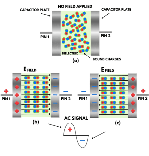
Another important concept is that when a signal edge propagates, since the leading edge represents a change in the electromagnetic field, it generates a displacement current in the dielectric between the two conductors. This phenomenon is explained by Maxwell’s equations (particularly the Ampere-Maxwell laws) summarized by Oliver Heaviside. The most way to understand this is to imagine the current flow when an AC power source is applied to a capacitor (see Figure 2).

Figure 2: Capacitor (a) No electric field applied (b) Positive electric field applied (c) Negative electric field applied
In reality, there is no conduction current between the capacitor plates and the dielectric. However, the bound charges in the dielectric are polarized (displaced) by the electric field applied by the plates, making it appear as if a conduction current is flowing through the capacitor plates. The concept of displacement current is important because it explains how current forms during signal propagation, especially before reaching a load. Classical circuit theory states that current always flows in a loop. So why does current exist before the signal reaches the load, before a continuous conduction current loop from the source to the load and back to the source is established? It is precisely because of the displacement current that the current can continue to flow in a loop during signal propagation. If only conduction current existed without displacement current, the signal would not propagate—because a current loop formed by conduction current alone cannot be closed before reaching the load. This means that the conduction current must flow through the dielectric, which is, by definition, impossible. However, thanks to the “apparent current” of displacement current, the loop is instantaneously closed as the signal propagates.
The combination of conduction current and displacement current forms a current loop that propagates along the signal edge. As shown in Figure 3, this current loop can be divided into three parts:
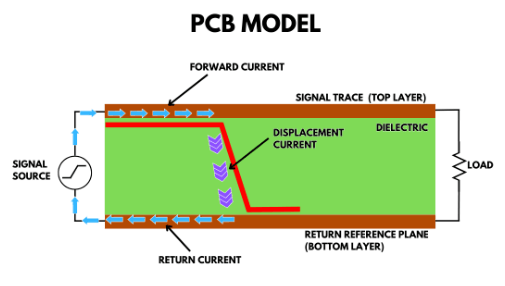
Figure 3: Current Loop and Displacement Current
Forward current: Flows in the top conductor in the direction of the signal toward the load.
Return current: Flows in the bottom conductor in the opposite direction of the signal back to the source.
Displacement current: Bridges the other two current components by “flowing” through the dielectric between the conductors and following the signal edge.
Confining Signal Energy to Control EMI
Managing the electromagnetic field between conductors and controlling the current path are critical to designing PCBs that not only provide excellent performance but also maintain excellent electromagnetic compatibility and signal integrity (see Figure 4).
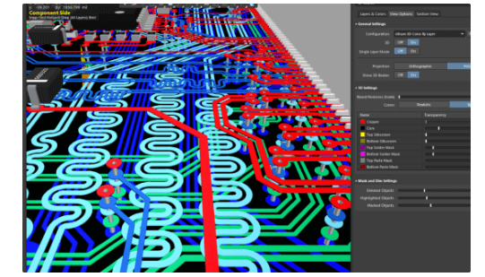
Figure 4: Example of an advanced PCB design using the Altium Designer 3D Viewer
This approach allows us to control radiated emissions at their source and avoid designing PCB structures that allow external interference to couple in.
In the next article in this series, we will discuss how to effectively reduce EMI by optimizing component layout.
Designing PCBs that meet high standards requires advanced tools that provide precise control over every aspect of the design. Altium Designer offers a comprehensive suite of PCB design layout and simulation capabilities to ensure that all requirements are met. An integrated design rules engine and online simulation tools verify compliance with specifications during the PCB routing process.
Once the design is complete, files can be seamlessly released to manufacturers using the Altium 365 platform, which simplifies collaboration and project sharing.