How to Achieve Efficient Automatic Routing for PCBs
Introduction
Printed Circuit Board (PCB) design has become increasingly complex with the advancement of electronic technologies. As circuit densities grow and signal speeds increase, the routing process has transformed from a manual task to a sophisticated automated operation. Efficient automatic routing is now essential for modern PCB design, offering significant time savings, improved accuracy, and better overall performance compared to manual methods.
This article explores the key strategies and techniques for achieving high-efficiency automatic routing in PCB design. We’ll examine the foundational preparation work, critical routing parameters, advanced techniques, post-routing optimization methods, and how to address common challenges in the automatic routing process.
Preparation for Automatic Routing
Proper Component Placement
The foundation of efficient automatic routing begins long before the routing process itself – with optimal component placement. Careful placement considering routing requirements can dramatically improve the success rate of automatic routing:
- Group related components together based on their functional relationships in the circuit
- Consider routing channels and leave adequate space between components
- Orient components to minimize crossing connections
- Place critical components first (connectors, processors, etc.)
- Consider thermal management requirements during placement
Layer Stack-up Design
An appropriate layer stack-up configuration is crucial for routing efficiency:
- Determine the optimal number of layers based on circuit complexity
- Assign clear purposes to each layer (signal, power, ground)
- Consider impedance control requirements for high-speed signals
- Plan for adequate ground return paths
- Ensure symmetry in the stack-up to prevent board warping
Design Rule Setup
Comprehensive design rules form the framework for successful automatic routing:
- Establish trace width rules based on current requirements
- Set appropriate clearance values between different net classes
- Define via styles and limitations
- Configure differential pair rules where applicable
- Set length matching tolerances for critical buses
- Establish topology rules for specific signal types
Key Parameters for Efficient Automatic Routing
Routing Strategy Selection
Modern EDA tools offer various routing strategies that significantly impact results:
- Grid-based vs. gridless routing: Gridless offers more flexibility but requires careful management
- Directional routing: Assigning primary directions to different layers (e.g., horizontal on odd layers, vertical on even)
- Fanout strategies: Determining how to escape from component pins
- Area routing: Defining specific approaches for dense component areas
Routing Order Prioritization
The sequence in which nets are routed affects overall success:
- Route power nets first (typically wider traces)
- Then route critical signals (clocks, differential pairs, sensitive analog)
- Follow with high-speed buses and other important signals
- Finally route less critical general signals
Via Management
Proper via usage is essential for efficient routing:
- Limit via counts to only what’s necessary
- Use appropriate via sizes for current requirements
- Implement via stitching where needed for thermal or EMI purposes
- Consider micro vias in HDI designs to increase routing density
- Establish via sharing rules for common connection points
Advanced Techniques for High-Efficiency Routing
Constraint-Driven Routing
Modern PCB tools allow sophisticated constraint definitions:
- Electrical constraints: Impedance, propagation delay, etc.
- Physical constraints: Length matching, meandering requirements
- Manufacturing constraints: DFM rules for reliability
- High-speed constraints: Crosstalk avoidance, EMI control
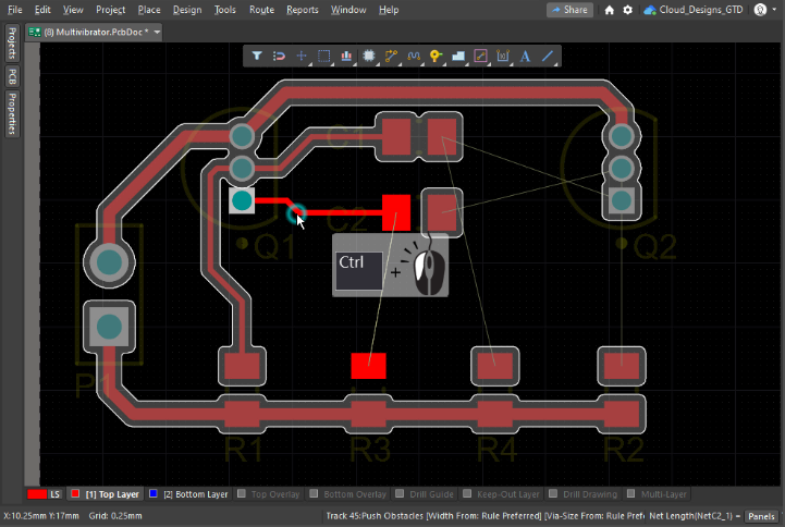
Interactive Routing Assistance
Combining automation with designer guidance:
- Guided routing: Letting the tool suggest paths while maintaining control
- Push-and-shove functionality for real-time obstacle avoidance
- Auto-completion of partially routed connections
- Conflict resolution suggestions during manual adjustments
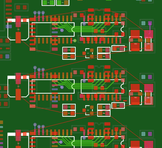
Bus Routing and Multi-Trace Routing
Efficient techniques for routing groups of related signals:
- Bus routing for parallel signal groups
- Differential pair routing with maintained spacing and length matching
- Length tuning through automatic meandering
- Phase matching for high-speed parallel interfaces
Reuse of Routing Patterns
Leveraging previous work for efficiency:
- Creating and using routing templates
- Repeating routing patterns across similar circuit blocks
- Saving and reusing successful routing solutions
- Parameterized routing cells for common configurations

Post-Routing Optimization
Design Rule Checking (DRC)
Comprehensive verification after automatic routing:
- Electrical rule verification
- Manufacturing rule compliance
- Signal integrity preliminary analysis
- Thermal consideration checks
Manual Clean-up and Optimization
Addressing areas where automatic routing may need refinement:
- Improving routing aesthetics where possible
- Reducing unnecessary vias and trace bends
- Optimizing power distribution for lower impedance
- Enhancing testability through pad access
Signal Integrity Verification
Ensuring the routed board meets performance requirements:
- Impedance verification for critical traces
- Crosstalk analysis for dense routing areas
- Timing analysis for high-speed interfaces
- Power integrity verification
Addressing Common Automatic Routing Challenges
Dealing with High-Density Designs
Strategies for complex, space-constrained layouts:
- Implementing HDI techniques (microvias, buried vias)
- Using thinner traces where electrically permissible
- Optimizing layer usage through careful planning
- Considering component placement adjustments
Handling Mixed-Signal Routing
Maintaining signal integrity in complex designs:
- Proper ground partitioning strategies
- Careful crossing management between analog and digital
- Appropriate spacing between sensitive signals
- Dedicated routing layers for critical signal types
Managing Thermal Considerations
Ensuring proper heat dissipation in routed designs:
- Incorporating thermal reliefs appropriately
- Using copper pours effectively for heat spreading
- Managing high-current traces to prevent hotspots
- Considering via placement for thermal conduction
Conclusion
Efficient automatic PCB routing is achievable through careful preparation, strategic parameter configuration, and the application of advanced routing techniques. By investing time in proper component placement, layer stack-up design, and comprehensive rule setup, designers can significantly improve automatic routing outcomes.
The key to success lies in understanding that automatic routing is not simply a “push button” operation, but rather a sophisticated process that requires thoughtful setup and occasional manual intervention. By combining the strengths of modern EDA tools with engineering expertise, PCB designers can achieve high-quality routing results with exceptional efficiency.
As PCB technologies continue to evolve, staying current with the latest automatic routing capabilities and methodologies will remain essential for maintaining competitiveness in electronic product development. The most successful designs will come from designers who master both the technical aspects of their EDA tools and the underlying electrical engineering principles that guide effective routing decisions.