How to Achieve Low-Cost PCB Design and Layout
Introduction
Printed Circuit Board (PCB) design and layout represent a significant portion of electronic product development costs. As electronics continue to permeate every aspect of modern life—from consumer gadgets to industrial equipment—the pressure to reduce PCB costs without compromising quality has never been greater. This article explores practical strategies for achieving low-cost PCB design and layout while maintaining functionality, reliability, and manufacturability.
The importance of cost-effective PCB design extends beyond simple budget considerations. For startups and small businesses, it can mean the difference between a viable product and an abandoned project. Even for established companies, optimizing PCB costs directly impacts profit margins and competitive pricing. By implementing smart design choices from the outset, engineers can significantly reduce both prototyping and production expenses.
Understanding PCB Cost Drivers
Before exploring cost-reduction techniques, it’s essential to understand what factors contribute most to PCB expenses:
- Board Size: Larger boards require more material and may reduce the number of panels that fit in manufacturing equipment.
- Layer Count: Each additional conductive layer increases material costs and manufacturing complexity.
- Materials: Standard FR-4 is most economical; specialized materials (high-frequency, high-temperature) cost more.
- Minimum Trace/Space: Tighter tolerances require more precise (and expensive) manufacturing processes.
- Hole Size and Count: More and smaller holes increase drilling time and may require laser drilling.
- Surface Finish: HASL is cheapest; ENIG, immersion silver, or gold add cost.
- Special Requirements: Impedance control, blind/buried vias, and other special features increase price.
- Quantity: Economies of scale apply—higher volumes reduce per-unit costs.
- Turnaround Time: Standard lead times are cheapest; expedited service adds premium.
Design Strategies for Cost Reduction
1. Optimize Board Size and Shape
Reducing board dimensions is one of the most effective ways to lower costs. Consider:
- Efficient Component Placement: Dense but manageable component arrangement minimizes board area.
- Standard Panel Sizes: Design to maximize panel utilization (common sizes: 18″×24″, 21″×24″).
- Board Shape: Rectangular boards without cutouts optimize material usage.
- Consider Smaller Form Factors: Evaluate if functionality can be achieved in a smaller footprint.
2. Minimize Layer Count
Each additional layer significantly impacts cost:
- Start with 2-Layer: Many designs can work with 2 layers with careful routing.
- Jump to 4-Layer Only When Necessary: 4-layer is about 30-40% more expensive than 2-layer.
- Avoid “Just in Case” Layers: Don’t add layers for hypothetical future needs.
- Use Advanced Routing Techniques: Creative routing can often eliminate need for extra layers.
3. Simplify PCB Specifications
Relaxing design specifications where possible reduces cost:
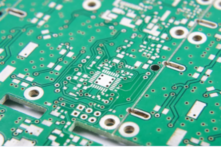
- Increase Minimum Trace/Space: 6/6 mil is standard; 8/8 mil or larger is cheaper.
- Use Larger Vias: ≥0.3mm mechanical drills are standard; smaller requires laser drilling.
- Standard Hole Sizes: Minimize unique drill sizes to reduce tool changes.
- Avoid Blind/Buried Vias: These require additional processing steps.
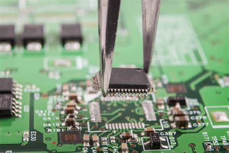
4. Component Selection and Placement
Component choices greatly influence total cost:
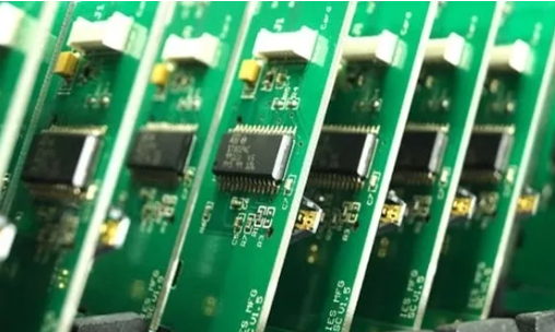
- Standard Packages: Use common packages (0805, SOIC, QFP) instead of exotic ones.
- Through-Hole vs. SMD: SMD components often allow smaller boards and automated assembly.
- Consolidate Parts: Use multifunction components when possible.
- Avoid Obsolete/End-of-Life Parts: These become expensive or unavailable.
- Consider Alternate Sources: Ensure components have second sources available.
5. Design for Manufacturability (DFM)
DFM reduces manufacturing difficulties and associated costs:
- Follow Manufacturer’s Guidelines: Each fab house has specific DFM rules.
- Standard Processes: Avoid special requirements unless absolutely necessary.
- Panelization: Design for efficient panelization if producing in volume.
- Testability: Include test points to reduce testing time/costs.
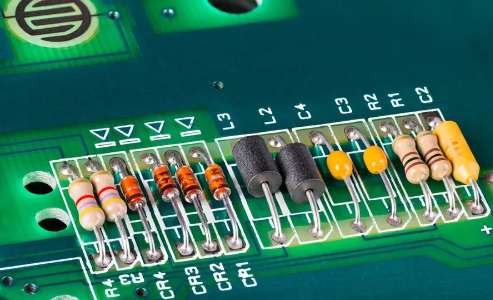
6. Smart Material Choices
- Standard FR-4: Suitable for most applications; avoid specialized materials unless required.
- 1oz Copper: Standard weight; heavier copper adds cost.
- Standard Thickness: 1.6mm is most economical; other thicknesses may cost more.
- Solder Mask Color: Green is standard; other colors may have minimum orders or higher costs.
Layout Techniques for Cost Savings
1. Efficient Routing Strategies
- Avoid Unnecessary Vias: Each via adds cost and potential reliability issues.
- Use Autorouter Judiciously: Manual routing often produces more efficient results.
- Optimize Power/Ground Planes: Good planning can reduce layer count.
- Minimize Crossovers: Careful component placement reduces routing complexity.
2. Thermal Management
- Natural Convection: Design for passive cooling when possible.
- Thermal Relief Pads: Proper use prevents soldering issues.
- Component Spacing: Adequate spacing reduces heat buildup.
3. EMI/EMC Considerations
- Proper Grounding: Good grounding prevents noise issues that might require fixes later.
- Signal Integrity: Careful routing prevents problems that might need shielding or redesign.
- Filter Placement: Strategic filter placement can reduce board complexity.
Prototyping and Production Considerations
1. Prototype Smartly
- Use Low-Cost Prototype Services: Many offer small quantities at reasonable prices.
- Virtual Prototyping: Simulate before building physical prototypes.
- Modular Design: Test critical sections separately before full board commit.
2. Volume Production Strategies
- Panelization: Proper panel design maximizes manufacturing efficiency.
- Standardization: Use consistent designs across product lines when possible.
- Supplier Relationships: Long-term relationships can yield better pricing.
3. Test and Validation
- Design for Test (DFT): Include test points to facilitate automated testing.
- Functional Testing: Plan testing procedures during design phase.
- Boundary Scan: Consider for complex boards to reduce test fixture costs.
Software and Tool Considerations
1. Cost-Effective Design Tools
- Open-Source Options: KiCad offers professional capabilities at no cost.
- Student Versions: Many commercial tools offer free or low-cost student editions.
- Online Tools: Browser-based tools can handle simple designs.
2. Library Management
- Create Custom Libraries: Standardize on frequently used components.
- Verify Footprints: Incorrect footprints lead to costly rework.
- Share Libraries: Team-wide libraries ensure consistency.
3. Design Reuse
- Modular Design: Create reusable circuit blocks.
- Version Control: Manage design iterations efficiently.
- Documentation: Proper documentation enables future reuse.
Common Pitfalls to Avoid
- Over-Engineering: Avoid specifications beyond what the application requires.
- Last-Minute Changes: These often lead to mistakes and rework.
- Ignoring DFM: Manufacturing difficulties increase costs.
- Component Obsolescence: Future redesigns add unexpected costs.
- Inadequate Testing: Field failures are the most expensive problems.
Case Studies
Case 1: Consumer Electronics Startup
A startup reduced their 4-layer IoT device to 2-layers by:
- Increasing board size slightly (18% larger)
- Using 8/8 mil trace/space instead of 6/6
- Careful component placement and routing
Result: 35% cost reduction, with minimal impact on functionality.
Case 2: Industrial Controller
An industrial equipment manufacturer saved costs by:
- Standardizing on 0.3mm minimum via size
- Limiting to 5 unique drill sizes (from 12 previously)
- Using green solder mask instead of blue
Result: 22% reduction in per-unit costs at volume.
Future Trends in Low-Cost PCB Design
- Advanced Design Tools: AI-assisted routing and optimization.
- New Materials: Lower-cost alternatives to traditional substrates.
- Additive Manufacturing: Potential for cost-effective small-run production.
- Embedded Components: May reduce layer count and assembly costs.
Conclusion
Achieving low-cost PCB design and layout requires a holistic approach that considers every stage from initial concept to volume production. By focusing on simplification, standardization, and manufacturability—while avoiding common pitfalls—engineers can significantly reduce costs without compromising quality. The key lies in making informed trade-offs between technical requirements and economic factors, always with an eye toward the entire product lifecycle.
Remember that the lowest-cost design isn’t necessarily the one with the cheapest upfront price tag, but rather the one that delivers required functionality at the optimal total cost of ownership. As PCB manufacturing technologies continue to evolve, staying informed about new materials, processes, and design techniques will enable even greater cost efficiencies in the future.