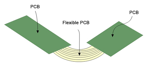
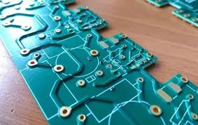
How to avoid electromagnetic problems in PCB design
In PCB design, electromagnetic compatibility (EMC) and related electromagnetic interference (EMI) have always been two major problems that engineers are worried about, especially in today’s situation where circuit board design and component packaging are constantly shrinking and OEMs require higher-speed systems. This article will share with you how to avoid electromagnetic problems in PCB design.
1.Crosstalk and routing are the key points
Tracing is particularly important to ensure the normal flow of current. If the current comes from an oscillator or other similar device, it is especially important to separate the current from the ground layer or not let the current run parallel to another trace. Two parallel high-speed signals will generate EMC and EMI, especially crosstalk. The resistance path must be minimized and the return current path must be as short as possible. The length of the return path trace should be the same as the length of the sending trace.
For EMI, one is called the “aggressor trace” and the other is the “victim trace”. Inductive and capacitive coupling will affect the “victim” trace due to the presence of electromagnetic fields, thereby generating forward and reverse currents on the “victim trace”. In this case, ripples will be generated in a stable environment where the length of the signal sent and received is almost equal.
In a well-balanced, stable routing environment, the induced currents should cancel each other out, eliminating crosstalk. However, we live in an imperfect world and this will not happen. Therefore, our goal must be to keep the crosstalk of all traces to a minimum. If the width between parallel traces is twice the width of the trace, the impact of crosstalk can be minimized. For example, if the trace width is 5 mils, the minimum distance between two parallel traces should be 10 mils or more.
As new materials and new components continue to emerge, PCB designers must also continue to deal with electromagnetic compatibility and interference issues.

2.Decoupling capacitors
Decoupling capacitors can reduce the adverse effects of crosstalk. They should be located between the power pins and ground pins of the device, which can ensure low AC impedance and reduce noise and crosstalk. In order to achieve low impedance over a wide frequency range, multiple decoupling capacitors should be used.
An important principle for placing decoupling capacitors is that the capacitor with the smallest capacitance value should be as close to the device as possible to reduce the inductive effect on the trace. This particular capacitor is as close as possible to the power pin or power trace of the device, and the pad of the capacitor is directly connected to the via or ground plane. If the trace is long, use multiple vias to minimize the ground impedance.
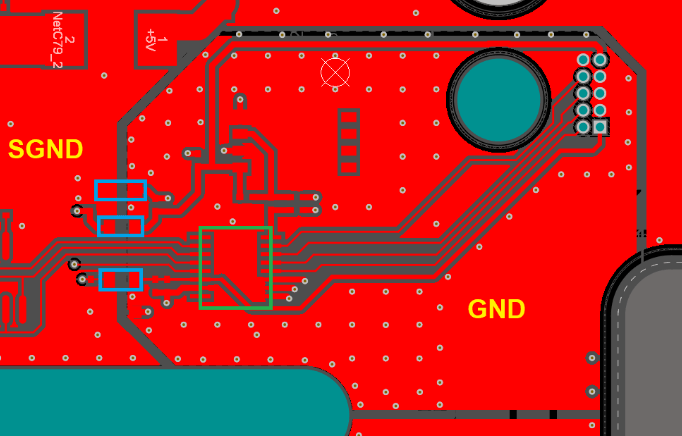
3.Ground the PCB
An important way to reduce EMI is to design the PCB ground plane. The first step is to make the ground area as large as possible within the total area of the PCB circuit board, which can reduce emissions, crosstalk and noise. You must be particularly careful when connecting each component to the ground point or ground plane. If you don’t do this, you can’t take full advantage of the neutralization effect of a reliable ground plane.
A particularly complex PCB design has several stable voltages. Ideally, each reference voltage has its own corresponding ground plane. However, if there are too many ground planes, the manufacturing cost of the PCB will increase, making the price too high. The compromise is to use ground planes in three to five different locations, each of which can contain multiple grounding sections. This not only controls the manufacturing cost of the circuit board, but also reduces EMI and EMC.
If you want to minimize EMC, a low-impedance grounding system is very important. In a multilayer PCB, it is better to have a reliable ground plane, rather than a copper thieving or scattered ground plane, because it has low impedance, provides a current path, and is the best reverse signal source.
The length of time the signal returns to the ground is also very important. The time for the signal to go back and forth to the signal source must be equal, otherwise it will produce an antenna-like phenomenon, making the radiated energy part of the EMI. Similarly, the traces that transmit current to/from the signal source should be as short as possible. If the length of the source path and the return path are not equal, ground bounce will occur, which will also generate EMI.
4.Avoid 90° angles
To reduce EMI, avoid 90° angles between traces, vias, and other components because right angles will generate radiation. The capacitance will increase at this corner, and the characteristic impedance will also change, resulting in reflections, which will cause EMI. To avoid 90° angles, traces should be routed to the corners at least at two 45° angles.
5.Use vias with caution
In almost all PCB layouts, vias must be used to provide conductive connections between different layers. PCB layout engineers need to be especially careful because vias create inductance and capacitance. In some cases, they can also create reflections because the characteristic impedance changes when a via is made in a trace.
It is also important to remember that vias increase the trace length and need to be matched. In the case of differential traces, vias should be avoided as much as possible. If they cannot be avoided, vias should be used in both traces to compensate for delays in the signal and return paths.
6.Cables and physical shielding
Cables carrying digital circuits and analog currents create parasitic capacitance and inductance, causing many EMC-related problems. If twisted-pair cables are used, the coupling level is kept low and the magnetic field generated is eliminated. For high-frequency signals, shielded cables must be used, with both the front and back sides grounded to eliminate EMI interference.
Physical shielding is to enclose the entire or part of the system with a metal package to prevent EMI from entering the PCB circuit. This shield is like a closed grounded conductive container that reduces the antenna loop size and absorbs EMI.