How to become an excellent hardware designer
When starting a hardware development project, the original driving force will come from many aspects, such as market needs, needs based on the entire system architecture, functional implementation needs of the application software department, needs to improve certain aspects of the system, etc.
Therefore, as a hardware system designer, you must take the initiative to understand the needs of various aspects, and combine them to propose the most appropriate hardware solution. For example, the original driving force of Project A came from a high-level software team within the company. They found in practice that the IP forwarding capabilities of the original processor board could not meet the requirements, which would cause great inconvenience to the configuration and use of the system, so they proposed the need for new hardware.
According to this goal, two high-performance network processors were selected in the hardware solution, and then in-depth communication with software designers was required to determine the memory size, internal structure, number and type of external interfaces and debugging interfaces, and other details. For example, software personnel like to completely separate the control signaling channel and the data channel, so careful consideration should be given when determining the direction of internal data.
At the beginning of the project, many discussion meetings need to be held.
All relevant departments should be invited to participate as much as possible. There are three benefits. First, we can fully understand everyone’s needs to avoid missing important functions in the system design. Second, we can let each department understand the situation of the project and prepare for time and personnel collaboration in advance. Third, from the emotional point of view, all departments are involved at the beginning of the design. This project has become a common fruit of everyone’s hard work, which will be cared for and well cooperated by everyone, which is very helpful for completing the work.
Issues to pay attention to in schematic design
There should be “take-it-ism” in schematic design. Nowadays, chip manufacturers can generally provide schematics of reference designs, so we should try to use these resources as much as possible, and make some of our own play on the basis of fully understanding the reference design. After the main chip is selected, the most critical peripheral design includes power supply, clock and interconnection between chips.
Power supply is the basis for ensuring the normal operation of the hardware system.
The design should be analyzed in detail: the power input that the system can provide; the power output that the single board needs to generate; the current size that each power supply needs to provide; the power circuit efficiency; the fluctuation range that each power supply can allow; the power-on sequence required by the entire power system, etc. For example, the network processor in Project A requires 1.25V as the core voltage, with an accuracy requirement between +5% and -3%, and a current of about 12A. According to these requirements, a 5V power input is used in the design, and a suitable power supply circuit is built using Linear’s switching power supply controller and IR’s MOSFET. The accuracy requirement determines the ESR selection of the output capacitor, and a remote feedback function is added to prevent voltage drops caused by excessive current.

The implementation of the clock circuit must take into account the jitter and other requirements of the target circuit.
GE’s PHY device is used in Project A. At the beginning, a zero-delay clock distribution chip with an internal phase-locked loop was used to provide a 100MHz clock. As a result, packet loss occurred on the GE link. Later, a simple clock buffer device was used to solve the packet loss problem. Analysis shows that the internal phase-locked loop introduced jitter.
The interconnection between chips must ensure the correct transmission of data.
In this regard, high-speed differential signal lines have the characteristics of high speed, good wiring, and good signal integrity. The interconnection between multiple chips in Project A all uses high-speed differential signal lines, and no problems occurred during debugging and testing.
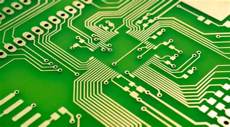
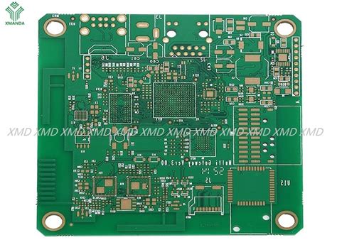
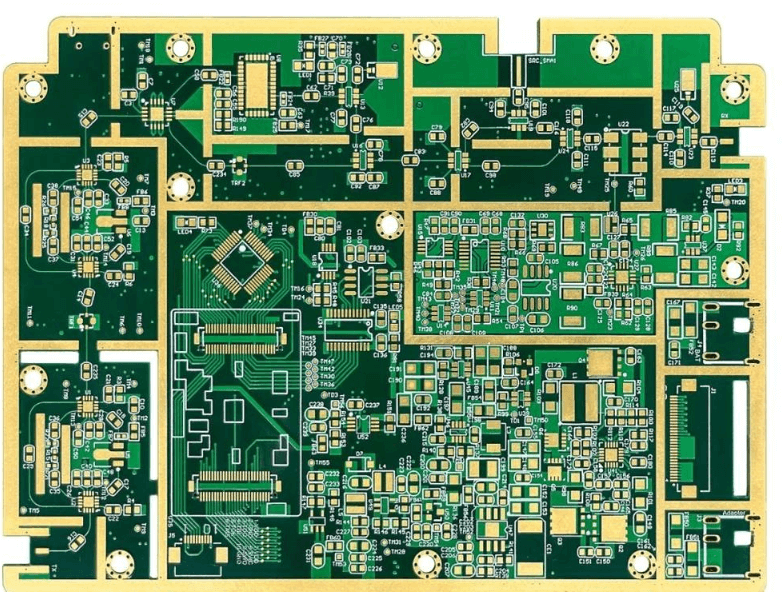
Issues to be aware of in PCB design
PCB design should have clear objectives. For important signal lines, the length of the wiring and the processing ground loop must be strictly required, while for low-speed and unimportant signal lines, they can be placed at a slightly lower wiring priority. Important parts include: power segmentation; length requirements for the clock line, control line and data line of the memory; wiring of high-speed differential lines, etc.
Project A uses memory chips to implement 1G DDR
Memory, the wiring for this part is very critical, and the topological distribution of the control line and the address line, the length difference control of the data line and the clock line, etc. must be considered. In the process of implementation, specific wiring rule requirements can be obtained based on the chip data sheet and the actual operating frequency, such as the length difference of the data line in the same group cannot exceed a certain number of mils, the length difference between each channel cannot exceed a certain number of mils, etc. When these requirements are determined, the PCB designer can be clearly required to implement them. If all the important wiring requirements in the design are clear, they can be converted into overall wiring constraints, and the automatic wiring tool software in CAD can be used to implement PCB design. This is also a development trend in high-speed PCB design.
Inspection and debugging
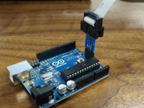
When preparing to debug a board, you must first carefully perform a visual inspection to check whether there are visible short circuits and pin tinning faults during the welding process, check whether there are problems such as incorrect placement of component models, incorrect placement of the first pin, missing assembly, etc., and then use a multimeter to measure the resistance from each power supply to the ground to check whether there is a short circuit. This good habit can avoid damaging the single board after rash power-on. You must have a calm mind during the debugging process. It is very normal to encounter problems. What you need to do is to make more comparisons and analyses, gradually eliminate possible causes, and firmly believe that “everything has a solution” and “there must be a reason for the problem”, so that you will be able to debug successfully in the end.
Some summary words
Now from a technical point of view, every design can be made in the end, but the success of a project depends not only on the technical implementation, but also on the completion time, product quality, and team cooperation. Therefore, good teamwork, transparent and honest project communication, meticulous R&D arrangements, and sufficient materials and personnel arrangements can ensure the success of a project.
A good hardware engineer is actually a project manager. He/she needs to obtain the requirements for his/her design from the outside world, and then summarize and analyze them into specific hardware implementations. He/she also needs to contact many chip and solution suppliers to select the appropriate solution. When the schematic is completed, he/she needs to organize colleagues to cooperate in review and inspection, and work with CAD engineers to complete the PCB design.
At the same time, he/she needs to prepare the BOM list, start purchasing and preparing materials, and contact the processing manufacturer to complete the board mounting.
During the debugging process, he/she needs to organize software engineers to work together on debugging, cooperate with test engineers to solve problems found in the test, and when the product is launched on site, if there is a problem, timely support is also required. Therefore, to be a hardware designer, you need to develop good communication skills, the ability to adjust to pressure, the ability to coordinate and make decisions to handle multiple matters at the same time, and a good and peaceful mentality, etc.
There is also carefulness and seriousness, because a small negligence in hardware design often causes very large economic losses.
For example, in the past, when the PCB design was completed and the manufacturing documents were issued, the power layer and the ground layer were connected together due to misoperation. After the PCB board was manufactured, it was directly mounted on the production line without inspection. The short circuit problem was not discovered until the test, but the components had already been soldered to the board, resulting in a loss of hundreds of thousands. Therefore, careful and serious inspection, responsible testing, unremitting learning and accumulation can enable a hardware designer to make continuous progress and then achieve some success in his career.