How to calculate the relationship between PCB line width and current
1.Calculation method
First calculate the cross-sectional area of the track. The copper foil thickness of most PCBs is 35um (if you are not sure, you can ask the PCB manufacturer, 1 ounce is 35um, but in fact it is less than 35um). Multiply it by the line width to get the cross-sectional area. Pay attention to convert it into square millimeters.
There is an empirical value of current density, which is 15~25 amperes/square millimeter. Weigh it by the cross-sectional area to get the current capacity. I=KT0.44A0.75 (K is the correction factor, generally 0.024 for the inner layer of the copper wire and 0.048 for the outer layer. T is the maximum temperature rise, in degrees Celsius (the melting point of copper is 1060℃). A is the cross-sectional area of the copper wire, in square MIL (not mm, note that it is square mil.). I is the maximum allowable current, in amperes (amp). Generally, 10mil=0.010inch=0.254 can be 1A, 250MIL=6.35mm, for 8.3A.
2.Data
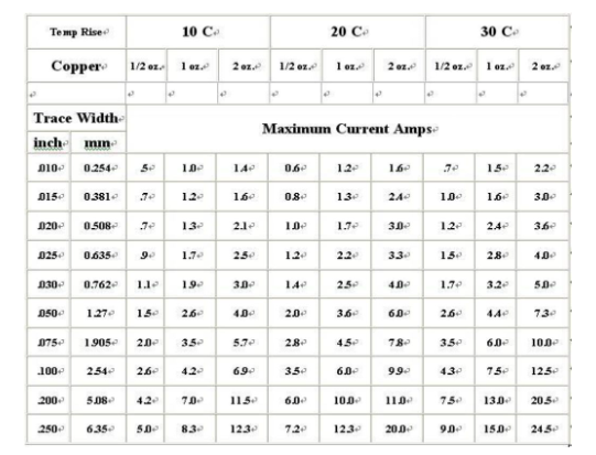
The calculation of PCB current carrying capacity has always lacked authoritative technical methods and formulas. Experienced CAD engineers can make more accurate judgments based on personal experience. However, for CAD novices, it is not a difficult problem. The current carrying capacity of PCB depends on the following factors: line width, line thickness (copper foil thickness), and allowable temperature rise. As we all know, PCB The wider the trace, the greater the current carrying capacity. Here, please tell me: Assuming that under the same conditions, a 10MIL trace can withstand 1A, how much current can a 50MIL trace withstand, is it 5A? The answer is naturally no. Please see the following data provided by international authoritative organizations: The unit of trace width is: Inch (inch = 25.4 millimetres) 1 oz. copper = 35 microns thick, 2 oz. = 70 microns thick, 1 OZ = 0.035mm 1mil. = 10-3inch. Trace Carrying Capacity per mil std 275
3.Experiment
In the experiment, the voltage drop caused by the line resistance generated by the wire length must also be considered. The tin on the process solder is only to increase the current capacity, but it is difficult to control the volume of tin. 1 OZ copper, 1mm wide, generally 1 – 3 A Ammeter, it depends on your line length and voltage drop requirements.
The maximum current value should refer to the maximum allowable value under the temperature rise limit, and the melting value is the value when the temperature rise reaches the melting point of copper. Eg. 50mil 1oz temperature rise 1060 degrees (i.e. copper melting point), the current is 22.8A.
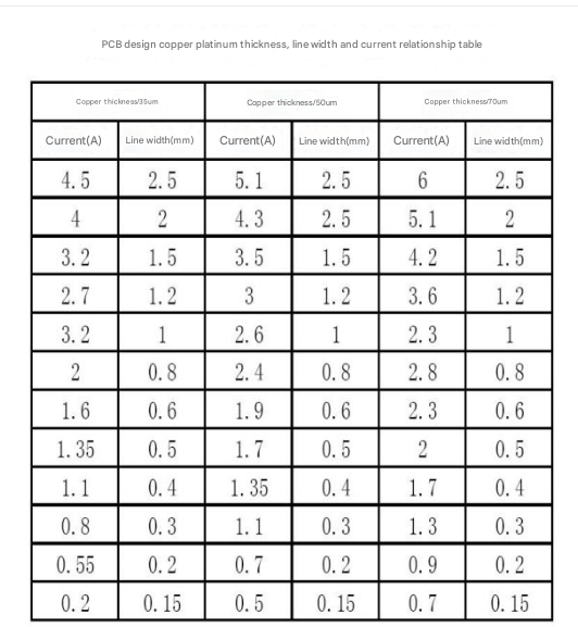
4.the relationship between copper platinum thickness, line width and current in PCB design
Before understanding the relationship between copper platinum thickness, line width and current in PCB design, let us first understand the conversion between ounces, inches and millimeters of PCB copper thickness: “In many data sheets, PCB copper thickness is often measured in ounces. Its conversion relationship with inches and millimeters is as follows:
1 ounce = 0.0014 inches = 0.0356 mm (mm)
2 ounces = 0.0028 inches = 0.0712 mm (mm)
Ounces are units of weight. The reason why they can be converted to millimeters is because pcb The copper thickness is ounces/square inch” PCB design copper platinum thickness, line width and current relationship table
The current carrying value of the wire is directly related to the number of vias and pads of the wire line (currently, there is no calculation formula for the influence of pads and vias per square millimeter on the carrying value of the line. Interested friends can find it by themselves. I am not very clear about it, so I will not explain it here). Here are some simple main factors that affect the current carrying value of the line.
- The carrying value listed in the table data is at room temperature 25 The maximum current carrying value that can be tolerated under the temperature, so in the actual design, various factors such as various environments, manufacturing processes, board processes, board quality, etc. must be considered. Therefore, the table is only provided as a reference value.
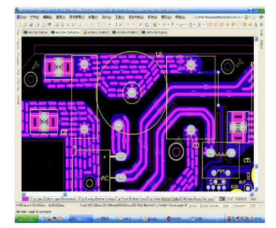
- In the actual design, each wire will also be affected by the pads and vias. For example, the wire segment with more pads will have its current carrying value greatly increased after tinning. Many people may have seen some sections of the line between the pads and the pads in some high-current boards being burned. The reason is very simple. After the pads are tinned, the current carrying value of that section of the wire is enhanced because of the component feet and solder. The maximum current carrying value of the pads between the pads is the maximum current carrying value allowed by the wire width. Therefore, when the circuit fluctuates instantly, it is easy to burn out the section of the line between the pads and the pads. The solution is to increase the wire width. If the board cannot allow the wire width to be increased, add a layer of Solder layer to the wire (generally, a 0.6-layer wire can be added to a 1 mm wire. Of course, you also add a 1 mm Solder layer wire) After tinning, this 1mm wire can be regarded as a 1.5mm~2mm wire (depending on the uniformity and amount of tin when the wire is tinned), as shown in the following figure:
This kind of processing method is not unfamiliar to those who are engaged in small household appliance PCB Layout. Therefore, if the amount of tinning is uniform enough and the amount of tin is large enough, this 1mm wire can be regarded as more than a 2mm wire. This is very important in single-sided high-current boards.
- The processing method around the pad in the figure is also to increase the uniformity of the current carrying capacity of the wire and the pad. This is especially important in boards with high-current thick pins (pins greater than 1.2 and pads above 3). Because if the pad is above 3mm and the pin is 1.2 Above, after tinning, the current of this pad will increase by dozens of times. If there is a large fluctuation in the high current, the current carrying capacity of the entire line will be very uneven (especially when there are many pads), and it is still easy to cause the possibility of burning the line between the pads. The treatment in the figure can effectively disperse the uniformity of the current carrying value of a single pad and the surrounding lines.
Finally, it is explained again: the current carrying value data table is only an absolute reference value. When there is no high current design, the data provided in the table can be increased by 10% to meet the design requirements. In general single-panel design, with a copper thickness of 35um, it can basically be designed at a ratio of 1 to 1, that is, a current of 1A can be designed with a 1mm wire, which can meet the requirements (calculated at a temperature of 105 degrees).
5.The relationship between copper foil thickness, trace width and current in PCB design
The current intensity of the signal. When the average current of the signal is large, the current that the wiring width can carry should be considered. The line width can refer to the following data:
PCB The relationship between copper foil thickness, trace width and current during design
The current carrying capacity of copper foils of different thicknesses and widths is shown in the table below:
How to calculate the relationship between PCB line width and current
Note:
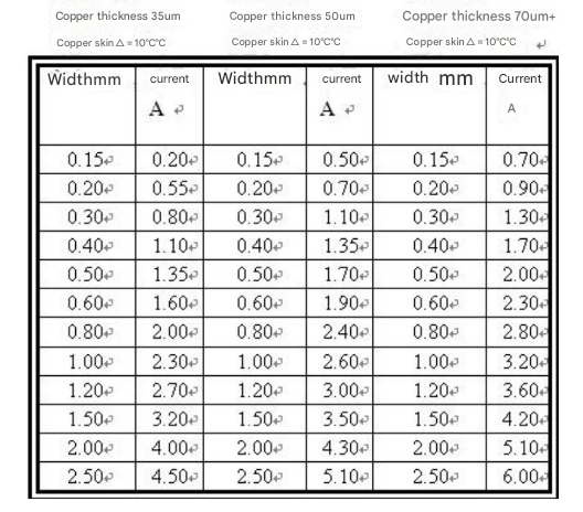
i. When using copper foil as a conductor to pass a large current, the current carrying capacity of the copper foil width should be selected and considered by referring to the value in the table and derated by 50%.
ii. In PCB design and processing, OZ (ounce) is often used as the unit of copper foil thickness. 1 OZ copper thickness is defined as the weight of copper foil in an area of 1 square foot, and the corresponding physical thickness is 35um; 2OZ copper thickness is 70um.
Excerpted from: Huawei PCB wiring specification internal data P10
6.Empirical formula
I=KT0.44A0.75
(K is the correction coefficient, generally 0.024 when the copper-clad wire is in the inner layer, and 0.048 when it is in the outer layer. T is the maximum temperature rise, in degrees Celsius (the melting point of copper is 1060℃)
A = is the cross-sectional area of copper, in square MIL (not mm, note that it is square mil.)
I is the maximum allowable current, in ampere (amp)
Generally, 10mil=0.010inch=0.254 can be 1A, 250MIL=6.35mm, for 8.3A
7. The calculation method provided by a netizen is as follows
First calculate the cross-sectional area of the track. The copper foil thickness of most PCBs is 35um (if you are not sure, you can ask the PCB manufacturer). It multiplied by the line width is the cross-sectional area. Note that it is converted into square millimeters. There is an empirical value of current density, which is 15~25 amperes/square millimeter. Weigh it by the cross-sectional area to get the current capacity.
8. A little experience about line width and via copper plating
When we draw PCBs, we generally have a common sense, that is, use thick lines (such as 50mil, or even more) for places with large currents, and use thin lines (such as 10mil). For some electromechanical control systems, sometimes the instantaneous current flowing through the trace can reach more than 100A, so thinner wires will definitely have problems.
A basic empirical value is: 10A/square mm, that is, the current value that can safely pass through a trace with a cross-sectional area of 1 square millimeter is 10A. If the line width is too thin, the trace will burn when a large current passes through. Of course, the current burning the trace must also follow the energy formula: Q=IIt. For example, for a trace with a current of 10A, a 100A current burr suddenly appears, and the duration is at the us level, then a 30mil wire can definitely withstand it. (At this time, another problem will arise-the stray inductance of the wire. This burr will generate a strong reverse electromotive force under the action of this inductance, which may damage other devices. The thinner and longer the wire, the greater the stray inductance, so in practice, the length of the wire must be considered comprehensively)
General PCB When drawing software is laying copper on the via pads of device pins, there are often several options: right-angle spokes, 45-degree spokes, and straight laying. What is the difference between them? Novices often don’t care much and just choose one that looks good. In fact, it is not. There are two main considerations: one is that the heat dissipation should not be too fast, and the other is that the overcurrent capability should be considered.
The characteristic of using the straight laying method is that the pad has a strong overcurrent capability, and this method must be used for device pins on high-power circuits. At the same time, its thermal conductivity is also very strong. Although it is good for device heat dissipation, it is a problem for circuit board welders, because the pad heats up too fast and it is not easy to tin. It is often necessary to use a larger wattage soldering iron and a higher welding temperature, which reduces production efficiency. The use of right-angle spokes and 45-degree spokes will reduce the contact area between the pin and the copper foil, slow heat dissipation, and make welding much easier. Therefore, the connection method for laying copper on the via pad should be based on the application scenario, and the comprehensive overcurrent capability and heat dissipation capability should be considered together. Do not use straight laying for low-power signal lines, and straight laying must be used for pads that pass large currents. As for right angles or 45 degree angle looks good.
Why do I bring this up? Because I was researching a motor driver a while ago. The H-bridge components in this driver kept burning out, and I couldn’t find the cause for four or five years. After a lot of hard work, I finally found out that the pad of a component in the power circuit used a copper plating method of right-angle spokes when plating copper (and because the copper plating was not well drawn, there were only two spokes in fact). This greatly reduced the overcurrent capacity of the entire power circuit. Although the product has no problems during normal use and works completely normally under 10A current. However, when the H-bridge is short-circuited, a current of about 100A will appear in the circuit, and the two spokes will burn out instantly (uS Then, the power circuit becomes open circuit, and the energy stored in the motor is dissipated through all possible channels without a discharge channel. This energy will burn the current measuring resistor and related operational amplifier components, destroy the bridge control chip, and penetrate into the signal and power supply of the digital circuit part, causing serious damage to the entire device. The whole process is as thrilling as using a hair to detonate a large landmine.