How to choose surface treatment for PCB printed circuits
Circuit materials rely on high-quality conductors and dielectric materials to connect modern complex components to each other for optimal performance. However, these PCB copper conductors, whether DC or millimeter wave PCB boards, need anti-aging and oxidation protection. This protection can be achieved in the form of electrolytic and immersion coatings. They usually provide different degrees of solderability, so even with ever-smaller components and micro surface mount (SMT), they can form very complete solder joints. There are many plating and surface treatments that can be used on PCB copper conductors in the industry. Understanding the characteristics and relative costs of each plating and surface treatment can help us make the right choice to achieve the highest performance and longest service life of the PCB board.
The selection of the final surface treatment of the PCB is not a simple process, and the purpose and working conditions of the PCB need to be considered. At present, PCBs are developing towards densely packed, small-pitch high-speed PCB circuits and smaller, thinner, and high-frequency PCBs.
This development trend has brought challenges to many PCB manufacturers.
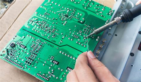
The production process of PCB circuits is that the material manufacturer provides laminates with different copper foil weights and thicknesses to the PCB manufacturer, and then the PCB manufacturer processes these laminates into various types of PCBs for use in electronic products. Without some form of surface protection, the conductors on the circuit will oxidize during storage. Conductor surface treatment acts as a barrier to isolate the conductor from the environment, not only protecting the PCB conductor from oxidation, but also providing an interface for soldering circuits and components, including wire bonding of integrated circuits (ICs).
The right surface treatment should help meet the application of the PCB circuit and the manufacturing process.
Due to different material costs, the processing and type of surface treatment required are different, so its cost is also different. Some surface treatments can provide high reliability and high isolation of circuits with dense routing, while other treatments may form unnecessary bridges between conductors. Some surface treatments can meet military and aerospace requirements such as temperature, shock and vibration, while others cannot guarantee the high reliability required for these applications. Here are some PCB surface treatments that can be used for circuits ranging from DC to millimeter wave bands and high-speed digital (HSD):
▪ Chemical nickel-gold (ENIG)▪ Chemical nickel-palladium-gold (ENEPIG)▪ Hot air leveling (HASL)▪ Chemical silver▪ Chemical tin▪ Lead-free tin spray (LFHASL)▪ Organic solderability protection film (OSP)▪ Electrolytic hard gold▪ Electrolytic bondable soft gold.
1.Chemical nickel-gold (ENIG)
ENIG, also known as chemical nickel-gold process, is a widely used surface treatment for PCB conductors. This is a relatively simple and low-cost process that forms a nickel layer on the surface of the conductor and then forms a thin layer of solderable gold on the nickel layer, forming a flat surface with good solderability even on densely packed circuits. Although the ENIG process ensures the integrity of the plated through hole (PTH), it also increases the loss of the conductor at high frequencies. This process has a long shelf life and complies with RoHS standards. It can provide long-term protection for PCB conductors from the completion of processing by circuit manufacturers to the component assembly process and the final product, so it has become a common surface treatment selected by many PCB developers.
2.Chemical nickel palladium gold (ENEPIG)
ENEPIG is an upgrade of the ENIG process, adding a thin layer of palladium between the chemical nickel layer and the gold plating layer. The palladium layer protects the nickel layer (the nickel layer protects the copper conductor), while the gold layer protects both palladium and nickel. This surface treatment is very suitable for wire bonding of devices to PCBs and can cope with multiple reflow processes. Like ENIG, ENEPIG also complies with RoHS standards.
3.Chemical silver
Chemical silver is also a non-electrolytic chemical process that attaches silver to the copper surface by completely immersing the PCB in a silver ion solution. Compared with ENIG, the coating formed by this process is more consistent and uniform, but lacks the protection and durability provided by the nickel layer in ENIG. Although its surface treatment process is simpler and more cost-effective than ENIG, it is not suitable for long-term storage at the circuit manufacturer.
4.Chemical immersion tin
The chemical immersion tin process forms a thin tin plating on the conductor surface through a multi-step process, including cleaning, micro-etching, acid solution pre-immersion, immersion in non-electrolytic tin solution and final cleaning. The tin treatment can provide good protection for copper and conductors, which contributes to the low-loss performance of HSD circuits. Unfortunately, due to the effect of tin on copper over time (i.e., one metal diffuses into another metal, which will reduce the long-term performance of circuit conductors), chemical immersion tin is not one of the conductor surface treatments with the longest service life. Like chemical immersion silver, chemical tin is also a lead-free and RoHS-compliant process.
5.Organic solderability protection film (OSP)
Organic solderability protection film (OSP) is a non-metallic protective layer applied by a water-based solution. This surface treatment is also RoHS-compliant. However, this surface treatment does not have a long shelf life and is best applied before the circuit and device are soldered to the PCB. Recently, new OSP films have appeared on the market, which are believed to provide long-term and permanent protection for conductors.
6.Electrolytic hard gold
Hard gold treatment is an electrolytic process that complies with the RoHS process flow, which can protect PCBs and copper conductors from oxidation for a long time. However, due to the high material cost, it is also one of the most expensive surface coatings. In addition, its solderability is poor, and the solderability of bondable soft gold treatment is also poor. It complies with the RoHS standard and can provide a good surface for wire bonding between devices and PCBs.
The selection of PCB surface treatment involves many factors, including application requirements and expected use conditions. It is not easy to make a suitable choice from these options. The advice of circuit material suppliers and circuit manufacturers can help us simplify this selection process. For environmental protection, most processes are RoHS-compliant. However, due to the different operating frequencies and speeds of the circuit, different surface treatment processes will have different effects on circuit performance. Therefore, listening to the advice of material suppliers and circuit manufacturers can further ensure that the PCB circuit achieves the performance goals of long-term use.