How to Create PCB Components and Component Libraries
Introduction
Printed Circuit Board (PCB) design is a fundamental skill in electronics engineering, and at the heart of every PCB design lies the component library. Creating accurate PCB components and well-organized component libraries is essential for efficient circuit design, reducing errors, and ensuring manufacturability. This comprehensive guide will walk you through the entire process of creating PCB components and building effective component libraries using modern electronic design automation (EDA) tools.
Understanding PCB Components
What Constitutes a PCB Component?
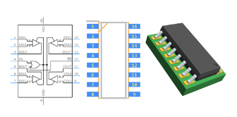
A complete PCB component consists of two primary elements:
- Schematic Symbol: The graphical representation used in circuit diagrams
- Footprint (PCB Decal): The physical representation of the component on the PCB
Additionally, a component may include:
- 3D models for mechanical verification
- Electrical parameters (pin numbers, pin types)
- Part information (manufacturer, part number, description)
- Simulation models
Types of PCB Components
- Through-hole components: Have leads that go through holes in the PCB
- Surface-mount devices (SMD): Mount directly onto the surface of the PCB
- Ball Grid Array (BGA): High-density packages with solder balls underneath
- Connectors and electromechanical components
Preparing to Create Components
Gathering Necessary Information
Before creating any component, collect all relevant documentation:
- Datasheets: Obtain the manufacturer’s datasheet for accurate dimensions
- Packaging information: Note package type (SOIC, QFP, etc.) and dimensions
- Pin configurations: Verify pin numbers and functions
- Recommended PCB land patterns: Many datasheets include these
Standardization Considerations
Establish consistent standards for your library:
- Naming conventions
- Grid settings
- Layer usage
- Text styles and sizes
- Reference designator prefixes
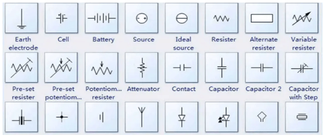
Creating Schematic Symbols
Best Practices for Schematic Symbols
- Logical representation: Group pins functionally rather than physically
- Clear labeling: Include pin names and numbers
- Proper sizing: Make symbols large enough to be readable but not excessive
- Consistent orientation: Inputs on left, outputs on right, power at top, ground at bottom
- Visible pin electrical types: Distinguish power, input, output, bidirectional pins
Step-by-Step Symbol Creation
- Open your EDA tool’s symbol editor
- Create a new symbol and assign the correct reference designator prefix
- Draw the symbol body using lines and shapes
- Add pins with proper numbers, names, and electrical types
- Add text labels for component values
- Set the origin point for proper placement
- Save the symbol with a descriptive name following your naming convention
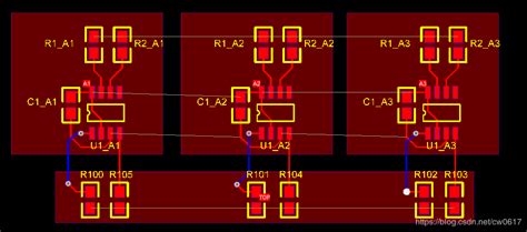
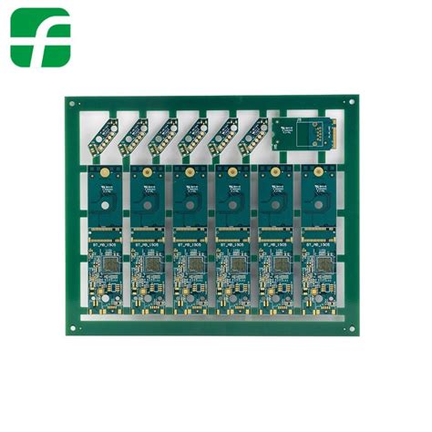
Creating PCB Footprints
Footprint Design Considerations
- Accurate dimensions: Follow datasheet specifications precisely
- Pad sizes: Account for manufacturing tolerances
- Solder mask and paste mask: Define appropriate openings
- Silkscreen markings: Include component outlines and polarity indicators
- Courtyard area: Define keep-out areas for adjacent components
- 3D model association: Link mechanical models when available
Step-by-Step Footprint Creation
- Open your EDA tool’s footprint editor
- Set the appropriate grid for the component size
- Place pads according to the package dimensions:
- For SMD: define pad shapes, sizes, and locations
- For through-hole: define drill sizes and pad diameters
- Add component outline on silkscreen layer
- Add reference designator text
- Define courtyard boundaries
- Set the origin point (typically pin 1 or component center)
- Save the footprint with a descriptive name following your naming convention
Building Component Libraries
Library Organization Strategies
- By component type: Resistors, capacitors, ICs, etc.
- By manufacturer: Useful when working with specific vendors
- By project: Dedicated libraries for specific designs
- By package type: SOT, QFP, BGA, etc.
Creating a Unified Component
In most EDA tools, you’ll need to:
- Create a new component in the library manager
- Associate the schematic symbol
- Assign one or more footprints
- Add component properties (value, tolerance, part number, etc.)
- Define pin mappings between symbol and footprint
- Add 3D models if available
- Save the complete component
Library Management Best Practices
- Version control: Use systems like Git to track changes
- Backup regularly: Maintain multiple copies of important libraries
- Documentation: Include README files explaining conventions
- Validation: Implement quality checks for new components
- Access control: Manage permissions for library editing
Advanced Component Creation Techniques
Creating Complex Components
For multi-part components (like multi-gate ICs):
- Divide the symbol into logical sections
- Assign section prefixes (U1A, U1B, etc.)
- Ensure proper power pin handling across sections
- Verify pin numbering consistency
Parametric Footprint Generation
Some EDA tools support parametric footprints:
- Create formulas based on standard package dimensions
- Automatically generate pads based on parameters
- Useful for standard packages like resistors, capacitors, and standard ICs
3D Model Integration
- Obtain STEP models from manufacturers or create your own
- Align 3D models precisely with 2D footprints
- Verify clearances in mechanical CAD tools
- Use for collision detection in PCB assembly
Quality Assurance and Validation
Component Verification Process
- Dimensional verification: Check against datasheet
- Pin mapping verification: Ensure symbol-to-footprint correctness
- Design rule check (DRC): Run automated checks
- Print verification: Print at 1:1 scale to check sizes
- Assembly test: Order sample PCBs with new components
Common Mistakes to Avoid
- Incorrect pin numbering
- Wrong pad sizes or spacing
- Missing or incorrect solder mask
- Inaccurate silkscreen markings
- Improper origin placement
- Inconsistent library organization
Maintaining and Updating Libraries
Library Maintenance Procedures
- Regular audits of existing components
- Update outdated footprints to current manufacturing capabilities
- Remove duplicate or obsolete components
- Verify manufacturer part availability
- Update component parameters as needed
Handling Component Revisions
- Document changes between revisions
- Maintain backward compatibility when possible
- Clearly mark obsolete components
- Communicate changes to all library users
Conclusion
Creating accurate PCB components and well-organized component libraries is a critical skill for electronics designers. By following systematic approaches to symbol and footprint creation, implementing consistent standards, and maintaining rigorous quality checks, you can build libraries that significantly improve your design efficiency and reliability. Remember that good library management is an ongoing process that pays dividends through reduced design errors, faster turnaround times, and improved manufacturing outcomes.
Investing time in proper component creation may seem tedious initially, but it forms the foundation for all your PCB designs. As you develop your libraries, you’ll create a valuable institutional knowledge base that can benefit your entire organization and streamline future design projects.