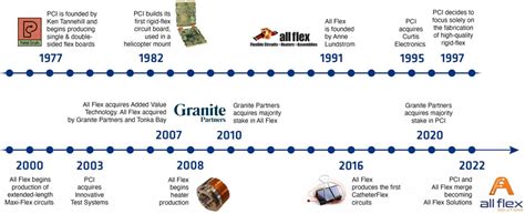
How to Design Hardware Circuits for PCB Testing Machines
Introduction
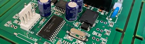
Printed Circuit Board (PCB) testing machines are essential tools in the electronics manufacturing industry, ensuring the quality and functionality of PCBs before they are deployed in final products. Designing the hardware circuits for these testing machines requires careful consideration of multiple factors including signal integrity, power distribution, measurement accuracy, and system reliability. This article provides a comprehensive guide on designing hardware circuits for PCB testing machines, covering key aspects from architecture planning to implementation details.
1. System Architecture Design
1.1 Understanding Testing Requirements
Before beginning the hardware design, clearly define the testing requirements:
- Types of tests to be performed (continuity, insulation, functional, etc.)
- Maximum number of test points
- Voltage and current requirements
- Signal frequency ranges
- Accuracy and resolution specifications
- Throughput requirements
1.2 Block Diagram Development
Create a system block diagram that includes:
- Main controller unit (typically an MCU or FPGA)
- Power supply subsystem
- Analog measurement circuits
- Digital signal generation and capture
- Switching matrix for test point routing
- Communication interfaces
- User interface components
2. Power Supply Design
2.1 Power Requirements Analysis
Calculate total power requirements considering:
- Controller and digital logic power needs
- Analog circuit power requirements
- Actuation power for relays or solid-state switches
- Margin for future expansion (typically 20-30%)
2.2 Power Distribution Network
Design considerations:
- Use separate regulators for analog and digital sections
- Implement proper decoupling (0.1μF ceramic capacitors near ICs)
- Consider low-noise LDOs for sensitive analog circuits
- Include protection circuits (overvoltage, reverse polarity)
- Implement proper grounding strategy (star ground for analog)
3. Analog Measurement Circuits
3.1 Continuity Testing Circuits
Design elements:
- Constant current source (typically 1-10mA)
- Precision voltage measurement
- Guard circuits for high-resistance measurements
- Four-wire Kelvin measurement for low-resistance tests
3.2 Insulation Resistance Testing
Key components:
- High-voltage generation (typically 100-1000V)
- Leakage current measurement
- Safety interlocks
- Discharge circuits for capacitive DUTs
3.3 Functional Test Analog Circuits
Design requirements:
- Programmable voltage/current sources
- Precision instrumentation amplifiers
- High-resolution ADCs (16-24 bits for measurements)
- Low-pass filtering for noise reduction
4. Digital Test Circuits
4.1 Digital Signal Generation
Implementation options:
- FPGA-based pattern generation
- Dedicated digital I/O controllers
- Level translation for different logic families
- Current limiting for protection
4.2 Digital Signal Capture
Design considerations:
- High-speed comparators
- Clock recovery circuits
- Timing measurement circuits
- Memory buffers for pattern storage
5. Switching Matrix Design
5.1 Switching Topology
Selection criteria:
- Crosspoint switches for maximum flexibility
- Tree or matrix configurations for cost optimization
- Mixed-signal switches for analog/digital routing
5.2 Switch Components
Options include:
- Electromechanical relays (high voltage/current)
- Reed relays (fast switching, moderate current)
- Solid-state analog switches (high speed, low current)
- MOSFET-based switches (custom solutions)
5.3 Switching Control
Design aspects:
- Driver circuits for relay coils
- Protection diodes for inductive loads
- Isolation between control and signal paths
- Sequencing control for safe operation
6. Controller and Interface Design
6.1 Main Controller Selection
Options and considerations:
- Microcontrollers for simple systems
- FPGAs for high-speed or parallel processing
- DSPs for complex signal processing
- Combination of above for mixed requirements
6.2 Communication Interfaces
Common implementations:
- USB for PC connectivity
- Ethernet for network integration
- GPIB or RS-232 for legacy systems
- Wireless options for mobile applications
6.3 User Interface
Design elements:
- Display interfaces (LCD, OLED)
- Tactile switches or touchscreen
- Status LEDs
- Audible indicators
7. Signal Integrity Considerations
7.1 PCB Layout Guidelines
Critical practices:
- Proper stack-up design (4-layer minimum recommended)
- Controlled impedance for high-speed signals
- Minimization of parallel trace lengths
- Careful routing of clock signals
7.2 Grounding and Shielding
Implementation techniques:
- Separate analog and digital grounds
- Proper use of guard rings
- Shielded enclosures for sensitive circuits
- Ferrite beads for noise suppression
7.3 EMI/EMC Considerations
Design approaches:
- Proper filtering at I/O connectors
- Compliance with relevant standards
- Radiated emissions testing
- Susceptibility hardening
8. Calibration and Self-Test
8.1 Calibration Circuits
Design features:
- Reference voltage sources
- Precision resistors for current scaling
- Built-in calibration switches
- Non-volatile memory for calibration data
8.2 Self-Test Capabilities
Implementation ideas:
- Loopback test paths
- Known-good reference components
- Power-on self-test routines
- Continuous monitoring of critical parameters
9. Safety Considerations
9.1 Electrical Safety
Essential protections:
- Fusing and current limiting
- Isolation barriers
- Emergency stop circuits
- Interlock switches
9.2 Operator Safety
Design requirements:
- Enclosure design considerations
- Clear warning labels
- Safety discharge circuits
- Compliance with relevant safety standards
10. Thermal Management
10.1 Heat Dissipation Analysis
Assessment factors:
- Power dissipation calculations
- Component derating
- Ambient temperature range
- Airflow requirements
10.2 Cooling Solutions
Implementation options:
- Passive heat sinking
- Forced air cooling
- Thermal vias in PCB
- Temperature monitoring circuits
Conclusion
Designing hardware circuits for PCB testing machines is a complex task that requires careful attention to multiple technical disciplines. By following a systematic approach that considers all aspects from system architecture to implementation details, designers can create robust, accurate, and reliable testing solutions. Key to success is maintaining signal integrity, ensuring measurement accuracy, and implementing proper safety measures throughout the design. As PCB technology continues to advance with higher densities and faster signals, testing machine designs must evolve accordingly, making the hardware design process both challenging and rewarding.
Remember that the specific implementation details will vary based on the exact requirements of your PCB testing application. Always prototype critical circuits and verify performance before finalizing the design. With careful planning and attention to detail, you can create a PCB testing machine that meets all your requirements for accuracy, reliability, and performance.