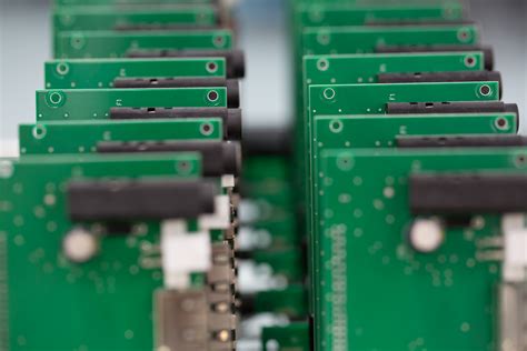
How to Design PCB Enclosures and Layouts to Avoid Interference
Designing printed circuit boards (PCBs) is both fun and challenging, but PCBs require enclosures for mechanical stability. PCB enclosures can be purchased off-the-shelf or custom designed using MCAD tools. Regardless of the method chosen to create the enclosure, the PCB layout must be imported into the MCAD tool to ensure that the board and components do not interfere with the enclosure.
When working with complex layouts, multi-board systems, or flexible PCBs, MCAD tools are essential for quickly checking for interference between the PCB enclosure, electronic components, and the board. Altium Designer provides the MCAD tools necessary for designing both the board and the enclosure, including mechanical interference checking, along with powerful board design features to support designers in creating complex circuit boards and accompanying enclosures for any application.
How to Design a PCB Enclosure and Layout to Avoid Interferences
When designing an enclosure around a PCB layout and preventing interference between components, there are several ways to ensure design accuracy:
Exporting the PCB layout as a STEP file and importing it into an MCAD application for enclosure design
Exporting the enclosure as a STEP file and importing it into a PCB design application
Altium Designer supports both of these processes as part of PCB layout and enclosure design. To prevent interference, you can import the STEP file into the PCB project and perform interference checks manually or automatically. By defining design rules, you can check for interference between the component layout and the PCB enclosure in 3D, helping you identify when components need to be moved on the PCB.
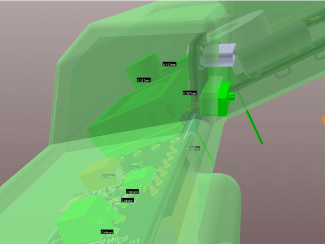
3D Clearance and Collision Checking with Altium Designer
Unfortunately, PCB designers require an MCAD designer or application to modify existing enclosures or create custom enclosures for PCB designs. These enclosure designs require a collaborative design approach between the electrical and mechanical domains.
Fully Custom PCB Enclosures Require Collaborative Design
For many products, creating an ideal user experience requires collaborative design between mechanical and electrical designers. The interaction between mechanical and electrical engineering disciplines offers two approaches to defining constraints within the design space:
Mechanical-first approach: The required enclosure is determined first and used as the primary constraint for board size, component size, and component placement.
Electrical-first approach: The PCB dimensions are determined first, sometimes finalized after layout is complete. Once layout is complete, the mechanical designer designs the enclosure around the PCB.
The electrical-first approach is simpler because it gives the electrical designer full freedom to select and place components on the PCB layout. Once completed, the mechanical engineer builds the enclosure based on the final design model. This is essentially a “waterfall” approach, similar to the traditional “bulk-and-wall” engineering model.
This type of design may appear simple; custom designs often resemble a box, essentially creating an enclosure with minimal margins around the PCB components.
When products require more unique functionality and aesthetics, a mechanical-first approach prevails. This means design teams need to adopt a collaborative design approach, initially defining constraints in the MCAD software rather than in the PCB layout.
MCAD Co-Design of PCB Enclosures
A key process in developing PCB enclosures is MCAD co-design, where mechanical and electrical designers iteratively develop the PCB and its enclosure. This process is suitable for complex PCB enclosures, which may have intricate shapes or even integrate multiple PCBs into the same assembly.
For mechanical engineers, MCAD co-design offers many advantages, not the least of which is the ability to define constraints for electrical designers. Setting constraints on a PCB layout means determining several key elements:
Overall PCB dimensions and specifications
Total PCB thickness
Location of keepout areas (including height-based keepout areas)
Location of mounting holes, cutouts, or slots
Placement of specific components (usually connectors)
Planning and modeling wiring and cable routing
Pre-planning these elements does place constraints on the board designer, but it also ensures that their design will meet the requirements of the target enclosure. After the layout is complete, a 3D model of the PCB with components is typically reviewed to check for fit within the enclosure.
Using Altium Designer’s integrated MCAD toolset, enclosure clearances and interferences can be checked in 3D.
Once these constraints are defined, the mechanical designer can focus on building the enclosure and planning the manufacturing process. Meanwhile, the PCB designer can focus on designing the PCB layout within these constraints. To ensure that the PCB layout does not violate mechanical constraints, component placement needs to be regularly reviewed. This can be accomplished through standard push-pull processes in cloud platforms like Altium 365.
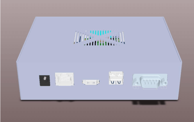
Off-the-Shelf PCB Enclosures
There are many off-the-shelf PCB enclosure options available with a variety of features, making them very useful in many scenarios, especially for prototyping or rapid production of low- to medium-volume products. These off-the-shelf enclosures offer a fast time-to-market option and are suitable for a wide range of designs. They often feature mounting posts, thermal relief holes, threaded fastener holes, cable or connector openings, and airflow vents. Some off-the-shelf enclosures may also have a high ingress protection (IP) rating. When combined with panel-mount or chassis-mount connectors of equivalent rating, this allows for the creation of a high-reliability system that can withstand harsh environments.
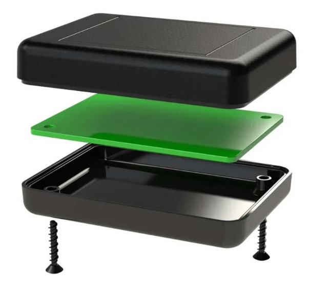
Below is an example of a PCB enclosure from Polycase, suitable for many designs, including digital systems, embedded systems, and small power electronics systems.
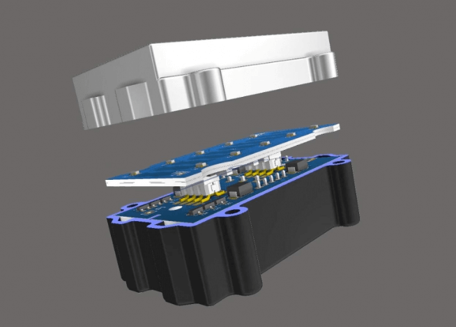
Off-the-shelf PCB enclosure suppliers typically provide a 3D mechanical model of the enclosure, which can be used to define the PCB constraints. Using the 3D enclosure model and deriving a 2D outline for the board follows an MCAD-first approach to PCB enclosure design and requires support from an MCAD software package. Based on the 3D model, the MCAD designer can create a PCB outline that fits within the enclosure and accommodates any mounting posts or legs. CAD users can also provide board thickness specifications within the enclosure model and pass this information to the PCB designer.
While transferring DXF files is often the standard method for defining board geometry, MCAD software users can also push board geometry directly to ECAD platforms like Altium Designer. Pushing directly to the PCB eliminates file exchange and ensures that designers always have the correct PCB mechanical specifications.
Handle Complex 3D PCB Layouts in Altium Designer
When working with complex layouts, multi-board systems, or flexible PCBs, you need MCAD tools to quickly check for interference between the PCB enclosure, electronic components, and the board. Altium Designer provides the MCAD tools you need to design both the board and the enclosure, including mechanical interference checking, along with powerful board design capabilities to create complex boards and their corresponding enclosures for any application.
Altium Designer is a PCB design platform that offers comprehensive ECAD and MCAD capabilities. Whether designing simple PCBs or complex multi-board systems, Altium Designer has the electrical and mechanical design capabilities you need to create cutting-edge technology.
Combining Altium Designer with Altium 365 brings a new level of integration to the electronics industry, previously only available in software development, enabling designers to work from home and achieve unprecedented productivity gains.